Logic gates are the basic building blocks of any digital system. It is an electronic circuit having one or more than one input and only one output. The relationship between the input and the output is based on a certain logic. Based on this, logic gates are named as AND gate, OR gate, NOT gate etc.
AND Gate
A circuit which performs an AND operation is shown in figure. It has n input (n >= 2) and one output.
Logic diagram
Truth Table
OR Gate
A circuit which performs an OR operation is shown in figure. It has n input (n >= 2) and one output.
Logic diagram
Truth Table
NOT Gate
NOT gate is also known as Inverter. It has one input A and one output Y.
Logic diagram
Truth Table
NAND Gate
A NOT-AND operation is known as NAND operation. It has n input (n >= 2) and one output.
Logic diagram
Truth Table
NOR Gate
A NOT-OR operation is known as NOR operation. It has n input (n >= 2) and one output.
Logic diagram
Truth Table
XOR Gate
XOR or Ex-OR gate is a special type of gate. It can be used in the half adder, full adder and subtractor. The exclusive-OR gate is abbreviated as EX-OR gate or sometime as X-OR gate. It has n input (n >= 2) and one output.
Logic diagram
Truth Table
XNOR Gate
XNOR gate is a special type of gate. It can be used in the half adder, full adder and subtractor. The exclusive-NOR gate is abbreviated as EX-NOR gate or sometime as X-NOR gate. It has n input (n >= 2) and one output.
Logic diagram
Truth Table
How to Get Started With Laser Cutting? – Beginners Guide
Laser Cutters are great tools offering the possibility to create many different things. From simple boxes to engraving detailed graphics into wood or building complex three-dimensional objects. In this beginners guide, I will explain the basics of how a laser cutter works, show you some examples of things that can be made with a laser and how to create designs for laser cutting or engraving. You’ll also learn which material can be used and how to get access to a laser cutter.
What is a laser cutter?
A laser cutter is a computer controlled machine that uses a laser beam to precisely cut or engrave material. A laser is basically just highly focused, highly amplified light. The laser beam causes the material to locally burn, melt or vaporize. The kind of material that a laser can cut depends on the type of laser and the specific machine’s power.
The term “Laser” is an acronym for “Light Amplification by Stimulated Emission of Radiation”. Laser technology was developed in the 1960s.
There are different types of laser cutters. This guide will focus on gas lasers and CO2 lasers in particular, as this type is most commonly used by hobbyists and small businesses. Other types are for example fiber or crystal lasers which are mostly used for industrial applications.
CO2 laser cutters are capable of cutting and engraving a wide range of non-metallic materials such as wood, paper, acrylic, textiles, and leather. For more materials and details look here.
How does a laser cutter work?
In a CO2 laser cutter machine, the laser beam is created in a tube filled with CO2 gas. Next, with the help of mirrors and lenses, the laser beam is directed to the laser head and focused on the material surface. Electronically controlled motors move the laser head to cut or engrave the desired shape into the material of the workpiece. The shape is defined by an input file which can be a vector or raster image.
When the laser hits the material, a very small area is heated in an extremely short period, causing the material to melt, burn or vaporize.
What can you do with a laser cutter?
In general, there are three tasks that a laser cutter can perform: Cutting, Engraving and Marking.
Cutting
When the laser beam goes all the way through the material of the workpiece it creates a cut. A laser cut is generally very precise and clean. The look of the cut edges depends on the material. For example, the edges of cut wood are typical of a darker brown than the original wood. The edges of acrylic do not change color and have a nice glossy finish after laser cutting.
The kerf of a laser cutter is very small. The term kerf refers to the width of the groove made while cutting. This varies from material to material and is also dependent on the specific settings of the laser. For many materials, the kerf will be somewhere between 0.05 mm (0.002 in) and 0.5 mm (0.02 in).
Engraving
It is called engraving when the laser beam removes parts of the top material but does not cut all the way through the material.
Marking
Marking is when the laser does not remove material but for example, changes the color of the material. With CO2 laser cutters marking is mostly used when working with metals. A marking solution (e.g. CerMark or Enduramark) is applied on the surface of the workpiece. After drying of the marking solution an engraving is performed. The heat from the laser bonds the solution to the metal, resulting in a permanent mark.
How to get started with laser cutting in 4 steps
So you want to laser cut your own design? Here’s a step-by-step overview of what you need to consider to make it happen.
In many cases the answer will be no – you don’t need to buy a laser cutter. There are a lot of other options to get access to a laser cutter:
Makerspaces
If you are interested in getting some hands-on experience with a laser cutter, I recommend looking for a local makerspace. Makerspaces – sometimes also called maker lab or hackerspace – are collaborative work spaces for making and learning. They offer a variety of equipment like for example 3D printers, CNC machines, soldering irons and very often also laser cutters!
The big advantage of makerspaces is that the other people there are usually very helpful and they often also offer courses on how to operate their machines. There are many different types of makerspaces some are non-profit, others operate based on memberships or charge fee for the usage of equipment. Check out if there is a makerspace nearby. The site themakermap.com is a good place to start looking.
Schools, colleges and universities
Especially if you are a student, schools, colleges and universities are also a good place to look for a laser cutter.
Laser cutting services
The third option is using a laser cutter service. When working with a laser cutting service you just send them your files, choose a material and then the company will do the cutting and ship the finished parts to you. Below you can find some online laser cutting services or just look for a local laser cutting shop.
If you are just starting with laser cutting I recommend trying one of the options above before looking into buying a laser cutter to get some experience and find out which features are most important for you.
Even when looking only at CO2 lasers, there is a wide variety of different laser machines available and the selection is continuously growing. The price range is big, with entry-level Chinese imports starting at about 500 EUR/USD and professional grade machines costing several 10,000 EUR/USD. In this guide, I won’t go into more details, but I plan to write an overview of the different types available on the market and the most important features to consider when buying a laser cutter, in a future post.
2. What materials can be cut or engraved with a laser?
CO2 laser machines are capable of cutting and engraving a variety of materials. However, there are also materials which cannot be processed. This may be because the laser can not cut through the material, or because toxic gases would form. Also, very flammable materials cannot be used.
Depending on the power and other specifications of the machine you are using, the maximal material thickness that can be cut will vary. The power of laser cutters is measured in Watt. Typical power levels range between 30 Watt and 120 Watt. Lasers with higher power are mostly used in industrial applications only.
Material
Cut
Engrave
Comment
Wood
x
x
Plywood
x
x
Lasers can struggle to cut plywood sheets with exterior glue. Use plywood with interior glue.
Materials that should not be cut or engraved with a laser
There are materials that should never be processed with a laser because this will lead to the creation of toxic gases or dust which can also damage the machine.
These materials include (but are not limited to):
Leather and artificial leather that contains chromium (VI)
Carbon fibers (Carbon)
Polyvinyl chloride (PVC)
Polyvinyl butyrale (PVB)
Polytetrafluoroethylenes (PTFE /Teflon)
Beryllium oxide
Any material containing halogens (fluorine, chlorine, bromine, iodine and astatine), epoxy or phenolic resins
3. How to create a design for laser cutting or engraving?
Most CO2 laser cutters work very much like your everyday inkjet printer. The laser cutter comes with specific drivers which convert an image from a computer into a format that the laser cutter can read.
When working with laser cutters it is important to know the difference between vector images and raster images. Both image file types can be processed but raster images can only be used for engraving and not for cutting.
A vector image stores all the lines and colors as mathematical formulas. Raster images are pixel based. Which means that the image is made up of many small squares. Vector images can be scaled up without any loss in quality whereas raster images will start to “pixelate” at a certain enlargement.
The first thing that should be considered is the size of your material / the maximal size that the laser bed can accommodate. This defines the maximum size of your design. In general, it is a good idea to set the work area to this size.
The color mode should be set to RGB. Different colors are usually used to specify different processes. For example, red could be used for all the parts that will be cut and black will be used for engraving.
Creating a file for laser cutting
As explained before, during a cutting operation, the laser fires a continuous beam at the material to slice through it. To know where to cut the laser machine needs a vector path as the input file. Only vector graphics with the smallest possible line thickness (this depends on the software you are using) will be cut by the laser. All other graphics, like solid shapes or thicker lines, won’t be cut.
When cutting out text or other complex shapes you to consider that unconnected middle parts – like the inside of an “O” – will fall out. Depending on your desired design you may want to prevent this. For text you could, for instance, use a stencil font where all the inside parts of the letters are connected to the outside parts.
Creating a file for laser engraving
When engraving with a laser one can distinguish between vector engraving and raster engraving. Vector engraving is basically the same as cutting with the only difference that for the engraving the power is lower so that the laser just removes parts of the material and does not cut through.
For raster engraving, the input file can either be a vector file or a raster image. During raster engraving, the image is engraved by the laser line by line, pixel by pixel. The process is similar to the way in which an inkjet printer applies ink, but instead of ink being applied, material is removed by the laser beam.
Engraving works for simple shapes as well as for complex images. Photos need to be turned into grayscale images to be engraved.
4. How to use a laser cutter?
Once you have your design ready, it is time for the final step – the cutting on the laser. Laser cutters are very powerful machines. You can create great things with them but they are also potentially dangerous, so first a word of warning. Before using a laser cutter always first make sure you read and understand all the safety instructions that come with it. In addition be aware that that wavelength of a CO2 laser is in the Infra-Red part of the light spectrum, so it is invisible to the human eye ye. The red dot you see with many machines on the material surface is only a positioning aid and not the laser beam that actually doing the cutting.
Preparation
First of all, check that your material fits inside the work area of the laser cutter and cut it to size if necessary. Also, be prepared to make some test cuts or engravings and bring some spare material with you.
You don’t necessarily need any extra tools when working with a laser cutter but in my experience, the following tool might come in handy:
Utility Knife: For cutting material that wasn’t cut all the way through by the laser cutter or to cut paper and cardboard to size.
Painter’s Tape/Masking Tape: Use it for masking the surface of your material to prevent burn stains and to tape down light materials.
Measurement Tape/Calipers: For measuring dimensions and making sure your final objects have the right size.
Settings
The four most important settings of a laser cutter are power, speed, frequency and for focus distance.
Power: Defines the output power of the laser. Typically can be set from 0 to 100% (maximum power). High power is used for cutting thick materials and lower power is used for engraving and cutting of thin materials such as paper.
Speed: Determines the movement speed of the laser head. For engraving and cutting of thin material, the speed is usually set (close) to the maximum.
Frequency (Hz, PPI): The frequency parameter specifies the number of laser pulses per second. Frequency depends completely on the material used. For example wood cuts best at around 500 to 1000 Hz and for acrylic 5000 to 20000Hz are recommended to achieve a smooth edge.
Focus: As previously explained, there is a focusing lens inside the laser head. The focus point (where the laser beam is thinnest) should be on the material surface or slightly below, for most applications. To ensure this the material needs to be a certain distance away from the lens. The exact distance depends on the type of focusing lens that is used. Many laser machines have a motorized bed which can be moved up and down to set the focus distance. Alternatively the position of the material surface a has to be manually adjusted.
So now that you have a basic understanding of the available settings you might ask yourself how to find the right settings for your projects? A good starting point is the laser cutter manual. Often you will find suggested settings for many materials. If you are working on a shared laser in a makerspace there are usually lists with recommended settings available.
Time to Cut!
Finally, you should be prepared to make your first cuts. It can take a few tries to find the ideal settings for your material. Always change only one parameter in a test process. For example, start with the power by testing different values in 5-10% increments. Once your are happy with your results, don’t forget to write down your settings for future reference.
WHAT IS 3D PRINTING?
THINKING ABOUT GETTING STARTED WITH 3D PRINTING BUT NOT SURE WHERE TO START? WHY NOT START AT THE BEGINNING AND ANSWER THE QUESTION – WHAT IS 3D PRINTING? READ ON AS WE GO OVER THE BASICS.
MakerBot 3D Printing Professional Solutions
INTRODUCTION TO 3D PRINTING
3D printing is a manufacturing technology that was invented in the 1980s. It has since evolved from being a rapid prototyping tool to full-fledged manufacturing technology. The evolution has been revolutionary leading to its adoption in a variety of sectors from automotive to aerospace, from healthcare to sports and from defense to fashion. The industrial term for 3D printing is additivemanufacturing since the material is continuously added to manufacture an object (as opposed to subtractive processes like cutting, milling, and machining). We introduce you to this rapidly growing revolutionary manufacturing technology.
WHAT IS 3D PRINTING?
MakerBot METHOD X 3D printer
In this section, we will share the answer to the question: “what is 3D printing?” As mentioned, 3D printing is a manufacturing technology that converts a CAD design into a three-dimensional solid object by successively laying down thin layers of materials one on top of another. In simple terms, it converts a virtual design into a physical object.
But 3D printing is not a single technology. It has several technologies that operate on the principle of additive manufacturing.
WHAT IS 3D PRINTING?
THE 3D PRINTING WORKFLOW
MakerBot enables 3D printing from anywhere with CloudPrint
The 3D printing workflow includes a series of steps that are essential to manufacturing an object. Below is the 3D printing workflow:
CAD Model: This is the first step towards 3D printing. It is the most vital element for 3D printing without which an object cannot be manufactured. A CAD model is created in a 3D modeling software (like Solidworks, Onshape, Rhino, etc.). Alternatively, a CAD model can also be obtained through reverse engineering by using a 3D scanner or through an online resource such as Thingiverse or GrabCAD. This CAD model is required to be compatible with 3D printing design rules to be able to be used for 3D printing.
Slicing Software: This is the second step in the 3D printing process and involves converting the CAD (or more often an STL file) into a file the 3D printer can read. The CAD model is imported into slicing software. The slicing software controls a range of parameters that can result in better 3D printing output. In most “slicers” you’ll find a visual representation of how the print will appear on the build plate so that you can properly orient it for best results. Some of the parameters that can be controlled are layer height, speed, temperature, raft layer adhesion, etc.
Original slicers were basic, but today slicers such as MakerBot CloudPrint are cloud-based and allow for not just print prep, but also remote monitoring of print process, job queuing, and reporting.
3D Print: This is the final step to complete the 3D printing process. The sliced file from the slicer software is sent to the 3D printer. Now with just the press of a button, the 3D printer will start printing the object in a layer by layer form until the object is complete and ready for retrieval or “harvesting”.
WHAT IS 3D PRINTING?
CATEGORIES OF 3D PRINTING
FDM 3D printing in process with MakerBot SR-30 material
The ASTM classifies all 3D printing technologies into seven categories namely material extrusion, vat photopolymerization, powder bed fusion, material jetting, binder jetting, directed energy deposition & sheet lamination. As we continue down the road of “what is 3D printing” here are some of the most popular technologies:
Fused Deposition Modeling (FDM) or Fused filament fabrication (FFF)
This is a material extrusion type of 3D printing technology. MakerBot is one of the leading manufacturers of FDM 3D printers and filaments. FDM 3D printers use thermoplastic polymer material in a filament form that is heated and deposited onto a build platform in a layer by layer form to form the complete object.
Stereolithography (SLA) & Digital light processing (DLP)
Stereolithography (SLA) was the first-ever patented 3D printing technology to be developed and commercialized. It falls under the vat photopolymerization category of 3D printing technology. It uses a photosensitive liquid resin material that is cured by a laser. The laser cures the resin point by point in a continuous process to ultimately form the entire object. Digital light processing (DLP) is a similar technology that uses projected UV light in place of a laser which can result in faster printing.
Selective Laser Sintering (SLS)
Selective Laser Sintering (SLS) is a powder bed fusion 3D printing technology that uses powdered polymer materials to form solid objects. This technology also uses a laser to sinter or melt the powder particles and fuse them to form the entire object.
Other technologies like Direct Metal Laser Sintering (DMLS), Selective Laser Melting (SLM), and Electronic Beam Melting (EBM) operate on a similar principle of powdered materials being fused with lasers (electron beam instead of a laser in case of EBM).
To understand the question of what is 3D printing, one must understand the materials that can be used in 3D printing. MakerBot manufactures a wide range ofFDM materials catering to all sorts of applications right from basic concept prototyping polymers like PLA to manufacturing-grade composite materials like carbon fiber. Let us take a look at some of these materials:
MODEL MATERIALS – POLYMERS
Polylactic acid (PLA):PLA is the most common FDM material. It is a biodegradable polymer material made from corn starch. PLA is a great material for early concept models because it is easy to use, office-friendly, and works great with breakaway supports which print faster and can be removed faster than dissolvable supports.
Acrylonitrile Butadiene Styrene (ABS):ABS is one of the most popular materials for injection-molded consumer products due to its clean surface finish, durability, and heat resistance. METHOD X can print manufacturing-grade ABS without warping and without weakening additives thanks to its 100°C heated chamber.
Nylon:Nylon is an excellent material for replacement parts in a manufacturing facility due to its high degree of abrasion resistance. It also has a relatively high impact strength and heat resistance further adding to its popularity with professionals. One drawback of Nylon is it may absorb moisture readily from the air which can lead to difficulty with both the filament and the printed part.
MODEL MATERIALS – COMPOSITES
Nylon 6 Carbon Fiber: Nylon 6 Carbon Fiber has the strength and lightweight benefits of other carbon fiber composites. The main thing about Nylon 6 that sets it apart from others in that category is its ability to withstand higher temperatures. The heat deflection temperature is significantly higher than many of the popular base polymers. In the case of MakerBot Nylon Carbon Fiber, the HDT is 100°C higher than that of ABS and 93°C higher than regular Nylon 6.
Nylon 12 Carbon Fiber: Much like Nylon 6 Carbon Fiber, the Nylon 12 variant has the benefits of strength, stiffness, and lightweight. Unlike Nylon 6, Nylon 12 has a better resistance to moisture uptake, making it somewhat easier to print and giving the printed part a cleaner final appearance without the need for post-processing. One drawback of Nylon 12 compared to Nylon 6 is it will generally have a lower HDT – so you really just need to weight what is most important for your specific application.
SUPPORT MATERIALS
Polyvinyl alcohol (PVA):PVA is a water-soluble support material that is compatible with many lower temperature model materials such as PLA and PETG. Because PVA is water-soluble it is very office-friendly and is a great option for printing the most complex geometries in a prototyping environment.
SR-30: SR-30 is a proprietary material developed by Stratasys to work seamlessly with ABS, ASA, and various other high-temp materials. Because of this focused development, using SR-30 with these typically more challenging materials can yield exceptional results that wouldn’t be possible with something like PVA, which is very difficult to use with ABS.
WHAT IS 3D PRINTING?
USES AND APPLICATIONS
Jamco America use the MakerBot METHOD 3D Printer to bring complex aircraft parts to market faster.
3D printing has developed into a powerhouse technology that has applications in wide-ranging fields. We see some of the popular applications as we continue to answer the question “what is 3D printing?”
Product Development
The ideal approach to new product development is through the design thinking principle but that cannot be applied as our current manufacturing methods do not allow us to iterate multiple ideas economically. It becomes difficult to spend huge amounts of money on the iteration phase. But 3D printing helps in rapidly and affordably iterate multiple product ideas. This helps in building a better customer-centric product.
In-house Manufacturing Aids
3D printing is the ideal technology to create customized manufacturing aids to improve in-house efficiencies in production and assembly stages. Customized aids like jigs & fixtures, guides, test gauges, maintenance tools, fit for purpose tools, etc., can be rapidly developed.
On-demand Manufacturing
Companies always have to be on their toes and the latest trend in manufacturing is on-demand manufacturing. 3D printing has significantly boosted this new approach to manufacturing. This not only delivers the product to the customer on time but also reduces the load on its warehouses and the associated investment in inventory.
Digital Manufacturing
Digital manufacturing is an extension of on-demand manufacturing wherein products can be manufactured right on-demand but through a website. The customer has to upload his CAD file and the 3D printer can use that file to rapidly 3D print the object as per the customer requirements.
Want to find out which is going to be the best fit for you and your organization? Talk to a MakerBot 3D printing expert today!
Relays
A relay is an electromagnetic switch operated by a relatively small electric current that can turn on or off a much larger electric current. The heart of a relay is an electromagnet (a coil of wire that becomes a temporary magnet when electricity flows through it). You can think of a relay as a kind of electric lever: switch it on with a tiny current and it switches on (“leverages”) another appliance using a much bigger current. Why is that useful? As the name suggests, many sensors are incredibly sensitive pieces of electronic equipment and produce only small electric currents. But often we need them to drive bigger pieces of apparatus that use bigger currents. Relays bridge the gap, making it possible for small currents to activate larger ones. That means relays can work either as switches (turning things on and off) or as amplifiers (converting small currents into larger ones).
How relays work
Here are two simple animations illustrating how relays use one circuit to switch on a second circuit.
When power flows through the first circuit (1), it activates the electromagnet (brown), generating a magnetic field (blue) that attracts a contact (red) and activates the second circuit (2). When the power is switched off, a spring pulls the contact back up to its original position, switching the second circuit off again.
This is an example of a “normally open” (NO) relay: the contacts in the second circuit are not connected by default, and switch on only when a current flows through the magnet. Other relays are “normally closed” (NC; the contacts are connected so a current flows through them by default) and switch off only when the magnet is activated, pulling or pushing the contacts apart. Normally open relays are the most common.
Here’s another animation showing how a relay links two circuits together. It’s essentially the same thing drawn in a slightly different way. On the left side, there’s an input circuit powered by a switch or a sensor of some kind. When this circuit is activated, it feeds current to an electromagnet that pulls a metal switch closed and activates the second, output circuit (on the right side). The relatively small current in the input circuit thus activates the larger current in the output circuit:
The input circuit (blue loop) is switched off and no current flows through it until something (either a sensor or a switch closing) turns it on. The output circuit (red loop) is also switched off.
When a small current flows in the input circuit, it activates the electromagnet (shown here as a dark blue coil), which produces a magnetic field all around it.
The energized electromagnet pulls the metal bar in the output circuit toward it, closing the switch and allowing a much bigger current to flow through the output circuit.
The output circuit operates a high-current appliance such as a lamp or an electric motor.
Relays in practice
Photo: Another look at relays. Top: Looking straight down, you can see the spring contacts on the left, the switch mechanism in the middle, and the electromagnet coil on the right. Bottom: The same relay photographed from the front.
Relays don’t always turn things on; sometimes they very helpfully turn things off instead. In power plant equipment and electricity transmission lines, for example, you’ll find protective relays that trip when faults occur to prevent damage from things like current surges. Electromagnetic relays similar to the ones described above were once widely used for this purpose. These days, electronic relays based on integrated circuits do the same job instead; they measure the voltage or current in a circuit and take action automatically if it exceeds a preset limit.
Other types of relays
What we’ve looked at so far are very general switching relays—but there are quite a few variations on that basic theme, including (and this is by no means an exhaustive list):
High-voltage relays: These are specifically designed for switching high voltages and currents well beyond the capacity of normal relays (typically up to 10,000 volts and 30 amps).
Electronic and semiconductor relays (also called solid-state relays or SSRs): These switch currents entirely electronically, with no moving parts, so they’re faster, quieter, smaller, more reliable, and last longer than electromagnetic relays. Unfortunately, they’re typically more expensive, less efficient, and don’t always work as cleanly and predictably (due to issues like leakage currents).
Timer and time-delay relays: These trigger output currents for a limited period of time (usually from fractions of a second to about 100 hours, or four days).
Thermal relays: These switch on and off to stop things like electric motors from overheating, a bit like bimetallic strip thermostats.
Overcurrent and directional relays: Configured in various different ways, these stop excessive currents from flowing in the wrong direction around a circuit (typically in power-generation, distribution, or supply equipment).
Differential protection relays: These trigger when there are current or voltage imbalances in two different parts of a circuit.
Frequency protection relays (sometimes called underfrequency and overfrequency relays): These solid-state devices trigger when the frequency of an alternating current is too high, too low, or both.
Post navigation
Transistors
Transistors make our electronics world go ’round. They’re critical as a control source in just about every modern circuit. Sometimes you see them, but more-often-than-not they’re hidden deep within the die of an integrated circuit. In this tutorial we’ll introduce you to the basics of the most common transistor around: the bi-polar junction transistor (BJT).
In small, discrete quantities, transistors can be used to create simple electronic switches, digital logic, and signal amplifying circuits. In quantities of thousands, millions, and even billions, transistors are interconnected and embedded into tiny chips to create computer memories, microprocessors, and other complex ICs.
There are two types of basic transistor out there: bi-polar junction (BJT) and metal-oxide field-effect (MOSFET). In this tutorial we’ll focus on the BJT, because it’s slightly easier to understand. Digging even deeper into transistor types, there are actually two versions of the BJT: NPN and PNP. We’ll turn our focus even sharper by limiting our early discussion to the NPN. By narrowing our focus down — getting a solid understanding of the NPN — it’ll be easier to understand the PNP (or MOSFETS, even) by comparing how it differs from the NPN.
Symbols, Pins, and Construction
Transistors are fundamentally three-terminal devices. On a bi-polar junction transistor (BJT), those pins are labeled collector (C), base (B), and emitter (E). The circuit symbols for both the NPN and PNP BJT are below:
The only difference between an NPN and PNP is the direction of the arrow on the emitter. The arrow on an NPN points out, and on the PNP it points in.
Transistor Construction
Transistors rely on semiconductors to work their magic. A semiconductor is a material that’s not quite a pure conductor (like copper wire) but also not an insulator (like air). The conductivity of a semiconductor — how easily it allows electrons to flow — depends on variables like temperature or the presence of more or less electrons. Let’s look briefly under the hood of a transistor. Don’t worry, we won’t dig too deeply into quantum physics.
A Transistor as Two Diodes
Transistors are kind of like an extension of another semiconductor component: diodes. In a way transistors are just two diodes with their cathodes (or anodes) tied together:
The diode connecting base to emitter is the important one here; it matches the direction of the arrow on the schematic symbol, and shows you which way current is intended to flow through the transistor.
The diode representation is a good place to start, but it’s far from accurate. Don’t base your understanding of a transistor’s operation on that model (and definitely don’t try to replicate it on a breadboard, it won’t work). There’s a whole lot of weird quantum physics level stuff controlling the interactions between the three terminals.
(This model is useful if you need to test a transistor. Using the diode (or resistance) test function on a multimeter, you can measure across the BE and BC terminals to check for the presence of those “diodes”.)
Transistor Structure and Operation
Transistors are built by stacking three different layers of semiconductor material together. Some of those layers have extra electrons added to them (a process called “doping”), and others have electrons removed (doped with “holes” — the absence of electrons). A semiconductor material with extra electrons is called an n-type (n for negative because electrons have a negative charge) and a material with electrons removed is called a p-type (for positive). Transistors are created by either stacking an n on top of a p on top of an n, or p over n over p.
Simplified diagram of the structure of an NPN. Notice the origin of any acronyms?
With some hand waving, we can say electrons can easily flow from n regions to p regions, as long as they have a little force (voltage) to push them. But flowing from a p region to an n region is really hard (requires a lot of voltage). But the special thing about a transistor — the part that makes our two-diode model obsolete — is the fact that electrons can easily flow from the p-type base to the n-type collector as long as the base-emitter junction is forward biased (meaning the base is at a higher voltage than the emitter).
The NPN transistor is designed to pass electrons from the emitter to the collector (so conventional current flows from collector to emitter). The emitter “emits” electrons into the base, which controls the number of electrons the emitter emits. Most of the electrons emitted are “collected” by the collector, which sends them along to the next part of the circuit.
A PNP works in a same but opposite fashion. The base still controls current flow, but that current flows in the opposite direction — from emitter to collector. Instead of electrons, the emitter emits “holes” (a conceptual absence of electrons) which are collected by the collector.
The transistor is kind of like an electron valve. The base pin is like a handle you might adjust to allow more or less electrons to flow from emitter to collector. Let’s investigate this analogy further…
Extending the Water Analogy
If you’ve been reading a lot of electricity concept tutorials lately, you’re probably used to wateranalogies. We say that current is analogous to the flow rate of water, voltage is the pressure pushing that water through a pipe, and resistance is the width of the pipe.
Unsurprisingly, the water analogy can be extended to transistors as well: a transistor is like a water valve — a mechanism we can use to control the flow rate.
There are three states we can use a valve in, each of which has a different effect on the flow rate in a system.
1) On — Short Circuit
A valve can be completely opened, allowing water to flow freely — passing through as if the valve wasn’t even present.
Likewise, under the right circumstances, a transistor can look like a short circuit between the collector and emitter pins. Current is free to flow through the collector, and out the emitter.
2) Off — Open Circuit
When it’s closed, a valve can completely stop the flow of water.
In the same way, a transistor can be used to create an open circuit between the collector and emitter pins.
3) Linear Flow Control
With some precise tuning, a valve can be adjusted to finely control the flow rate to some point between fully open and closed.
A transistor can do the same thing — linearly controlling the current through a circuit at some point between fully off (an open circuit) and fully on (a short circuit).
From our water analogy, the width of a pipe is similar to the resistance in a circuit. If a valve can finely adjust the width of a pipe, then a transistor can finely adjust the resistance between collector and emitter. So, in a way, a transistor is like a variable, adjustable resistor.
Amplifying Power
There’s another analogy we can wrench into this. Imagine if, with the slight turn of a valve, you could control the flow rate of the Hoover Dam’s flow gates. The measly amount of force you might put into twisting that knob has the potential to create a force thousands of times stronger. We’re stretching the analogy to its limits, but this idea carries over to transistors too. Transistors are special because they can amplify electrical signals, turning a low-power signal into a similar signal of much higher power.
Kind of. There’s a lot more to it, but that’s a good place to start! Check out the next section for a more detailed explanation of the operation of a transistor.
Operation Modes
Unlike resistors, which enforce a linear relationship between voltage and current, transistors are non-linear devices. They have four distinct modes of operation, which describe the current flowing through them. (When we talk about current flow through a transistor, we usually mean current flowing from collector to emitter of an NPN.)
The four transistor operation modes are:
Saturation — The transistor acts like a short circuit. Current freely flows from collector to emitter.
Cut-off — The transistor acts like an open circuit. No current flows from collector to emitter.
Active — The current from collector to emitter is proportional to the current flowing into the base.
Reverse-Active — Like active mode, the current is proportional to the base current, but it flows in reverse. Current flows from emitter to collector (not, exactly, the purpose transistors were designed for).
To determine which mode a transistor is in, we need to look at the voltages on each of the three pins, and how they relate to each other. The voltages from base to emitter (VBE), and the from base to collector (VBC) set the transistor’s mode:
The simplified quadrant graph above shows how positive and negative voltages at those terminals affect the mode. In reality it’s a bit more complicated than that.
Let’s look at all four transistor modes individually; we’ll investigate how to put the device into that mode, and what effect it has on current flow.
Note: The majority of this page focuses on NPN transistors. To understand how a PNP transistor works, simply flip the polarity or > and < signs.
Saturation Mode
Saturation is the on mode of a transistor. A transistor in saturation mode acts like a short circuit between collector and emitter.
In saturation mode both of the “diodes” in the transistor are forward biased. That means VBE must be greater than 0, and so must VBC. In other words, VB must be higher than both VE and VC.
Because the junction from base to emitter looks just like a diode, in reality, VBE must be greater than a threshold voltage to enter saturation. There are many abbreviations for this voltage drop — Vth, Vγ, and Vd are a few — and the actual value varies between transistors (and even further by temperature). For a lot of transistors (at room temperature) we can estimate this drop to be about 0.6V.
Another reality bummer: there won’t be perfect conduction between emitter and collector. A small voltage drop will form between those nodes. Transistor datasheets will define this voltage as CE saturation voltage VCE(sat) — a voltage from collector to emitter required for saturation. This value is usually around 0.05-0.2V. This value means that VC must be slightly greater than VE (but both still less than VB) to get the transistor in saturation mode.
Cutoff Mode
Cutoff mode is the opposite of saturation. A transistor in cutoff mode is off — there is no collector current, and therefore no emitter current. It almost looks like an open circuit.
To get a transistor into cutoff mode, the base voltage must be less than both the emitter and collector voltages. VBC and VBE must both be negative.
In reality, VBE can be anywhere between 0V and Vth (~0.6V) to achieve cutoff mode.
Active Mode
To operate in active mode, a transistor’s VBE must be greater than zero and VBC must be negative. Thus, the base voltage must be less than the collector, but greater than the emitter. That also means the collector must be greater than the emitter.
In reality, we need a non-zero forward voltage drop (abbreviated either Vth, Vγ, or Vd) from base to emitter (VBE) to “turn on” the transistor. Usually this voltage is usually around 0.6V.
Amplifying in Active Mode
Active mode is the most powerful mode of the transistor because it turns the device into an amplifier. Current going into the base pin amplifies current going into the collector and out the emitter.
Our shorthand notation for the gain (amplification factor) of a transistor is β (you may also see it as βF, or hFE). β linearly relates the collector current (IC) to the base current (IB):
The actual value of β varies by transistor. It’s usually around 100, but can range from 50 to 200…even 2000, depending on which transistor you’re using and how much current is running through it. If your transistor had a β of 100, for example, that’d mean an input current of 1mA into the base could produce 100mA current through the collector.
Active mode model. VBE = Vth, and IC = βIB.
What about the emitter current, IE? In active mode, the collector and base currents go into the device, and the IE comes out. To relate the emitter current to collector current, we have another constant value: α. α is the common-base current gain, it relates those currents as such:
α is usually very close to, but less than, 1. That means IC is very close to, but less than IE in active mode.
You can use β to calculate α, or vice-versa:
If β is 100, for example, that means α is 0.99. So, if IC is 100mA, for example, then IE is 101mA.
Reverse Active
Just as saturation is the opposite of cutoff, reverse active mode is the opposite of active mode. A transistor in reverse active mode conducts, even amplifies, but current flows in the opposite direction, from emitter to collector. The downside to reverse active mode is the β (βR in this case) is much smaller.
To put a transistor in reverse active mode, the emitter voltage must be greater than the base, which must be greater than the collector (VBE<0 and VBC>0).
Reverse active mode isn’t usually a state in which you want to drive a transistor. It’s good to know it’s there, but it’s rarely designed into an application.
Relating to the PNP
After everything we’ve talked about on this page, we’ve still only covered half of the BJT spectrum. What about PNP transistors? PNP’s work a lot like the NPN’s — they have the same four modes — but everything is turned around. To find out which mode a PNP transistor is in, reverse all of the < and > signs.
For example, to put a PNP into saturation VC and VE must be higher than VB. You pull the base low to turn the PNP on, and make it higher than the collector and emitter to turn it off. And, to put a PNP into active mode, VE must be at a higher voltage than VB, which must be higher than VC.
In summary:
Voltage relations
NPN Mode
PNP Mode
VE < VB < VC
Active
Reverse
VE < VB > VC
Saturation
Cutoff
VE > VB < VC
Cutoff
Saturation
VE > VB > VC
Reverse
Active
Another opposing characteristic of the NPNs and PNPs is the direction of current flow. In active and saturation modes, current in a PNP flows from emitter to collector. This means the emitter must generally be at a higher voltage than the collector.
If you’re burnt out on conceptual stuff, take a trip to the next section. The best way to learn how a transistor works is to examine it in real-life circuits. Let’s look at some applications!
Applications I: Switches
One of the most fundamental applications of a transistor is using it to control the flow of power to another part of the circuit — using it as an electric switch. Driving it in either cutoff or saturation mode, the transistor can create the binary on/off effect of a switch.
Transistor switches are critical circuit-building blocks; they’re used to make logic gates, which go on to create microcontrollers, microprocessors, and other integrated circuits. Below are a few example circuits.
Transistor Switch
Let’s look at the most fundamental transistor-switch circuit: an NPN switch. Here we use an NPN to control a high-power LED:
Our control input flows into the base, the output is tied to the collector, and the emitter is kept at a fixed voltage.
While a normal switch would require an actuator to be physically flipped, this switch is controlled by the voltage at the base pin. A microcontroller I/O pin, like those on an Arduino, can be programmed to go high or low to turn the LED on or off.
When the voltage at the base is greater than 0.6V (or whatever your transistor’s Vth might be), the transistor starts saturating and looks like a short circuit between collector and emitter. When the voltage at the base is less than 0.6V the transistor is in cutoff mode — no current flows because it looks like an open circuit between C and E.
The circuit above is called a low-side switch, because the switch — our transistor — is on the low (ground) side of the circuit. Alternatively, we can use a PNP transistor to create a high-side switch:
Similar to the NPN circuit, the base is our input, and the emitter is tied to a constant voltage. This time however, the emitter is tied high, and the load is connected to the transistor on the ground side.
This circuit works just as well as the NPN-based switch, but there’s one huge difference: to turn the load “on”, the base must be low. This can cause complications, especially if the load’s high voltage (VCC being 12V connecting to the emitter VE in this picture) is higher than our control input’s high voltage. For example, this circuit wouldn’t work if you were trying to use a 5V-operating Arduino to switch off a 12V motor. In that case, it’d be impossible to turn the switch off because VB (connecting to the control pin) would always be less than VE .
Base Resistors!
You’ll notice that each of those circuits uses a series resistor between the control input and the base of the transistor. Don’t forget to add this resistor! A transistor without a resistor on the base is like an LED with no current-limiting resistor.
Recall that, in a way, a transistor is just a pair of interconnected diodes. We’re forward-biasing the base-emitter diode to turn the load on. The diode only needs 0.6V to turn on, more voltage than that means more current. Some transistors may only be rated for a maximum of 10-100mA of current to flow through them. If you supply a current over the maximum rating, the transistor might blow up.
The series resistor between our control source and the base limits current into the base. The base-emitter node can get its happy voltage drop of 0.6V, and the resistor can drop the remaining voltage. The value of the resistor, and voltage across it, will set the current.
The resistor needs to be large enough to effectively limit the current, but small enough to feed the base enough current. 1mA to 10mA will usually be enough, but check your transistor’s datasheet to make sure.
Digital Logic
Transistors can be combined to create all our fundamental logic gates: AND, OR, and NOT.
(Note: These days MOSFETS are more likely to be used to create logic gates than BJTs. MOSFETs are more power-efficient, which makes them the better choice.)
Inverter
Here’s a transistor circuit that implements an inverter, or NOT gate:
An inverter built out of transistors.
Here a high voltage into the base will turn the transistor on, which will effectively connect the collector to the emitter. Since the emitter is connected directly to ground, the collector will be as well (though it will be slightly higher, somewhere around VCE(sat) ~ 0.05-0.2V). If the input is low, on the other hand, the transistor looks like an open circuit, and the output is pulled up to VCC
(This is actually a fundamental transistor configuration called common emitter. More on that later.)
AND Gate
Here are a pair of transistors used to create a 2-input AND gate:
2-input AND gate built out of transistors.
If either transistor is turned off, then the output at the second transistor’s collector will be pulled low. If both transistors are “on” (bases both high), then the output of the circuit is also high.
OR Gate
And, finally, here’s a 2-input OR gate:
2-input OR gate built out of transistors.
In this circuit, if either (or both) A or B are high, that respective transistor will turn on, and pull the output high. If both transistors are off, then the output is pulled low through the resistor.
H-Bridge
An H-bridge is a transistor-based circuit capable of driving motors both clockwise and counter-clockwise. It’s an incredibly popular circuit — the driving force behind countless robots that must be able to move both forward and backward.
Fundamentally, an H-bridge is a combination of four transistors with two inputs lines and two outputs:
Can you guess why it’s called an H bridge?
(Note: there’s usually quite a bit more to a well-designed H-bridge including flyback diodes, base resistors and Schmidt triggers.)
If both inputs are the same voltage, the outputs to the motor will be the same voltage, and the motor won’t be able to spin. But if the two inputs are opposite, the motor will spin in one direction or the other.
The H-bridge has a truth table that looks a little like this:
Input A
Input B
Output A
Output B
Motor Direction
0
0
1
1
Stopped (braking)
0
1
1
0
Clockwise
1
0
0
1
Counter-clockwise
1
1
0
0
Stopped (braking)
Oscillators
An oscillator is a circuit that produces a periodic signal that swings between a high and low voltage. Oscillators are used in all sorts of circuits: from simply blinking an LED to the producing a clock signal to drive a microcontroller. There are lots of ways to create an oscillator circuit including quartz crystals, op amps, and, of course, transistors.
Here’s an example oscillating circuit, which we call an astable multivibrator. By using feedback we can use a pair of transistors to create two complementing, oscillating signals.
Aside from the two transistors, the capacitors are the real key to this circuit. The caps alternatively charge and discharge, which causes the two transistors to alternatively turn on and off.
Analyzing this circuit’s operation is an excellent study in the operation of both caps and transistors. To begin, assume C1 is fully charged (storing a voltage of about VCC), C2 is discharged, Q1 is on, and Q2 is off. Here’s what happens after that:
If Q1 is on, then C1’s left plate (on the schematic) is connected to about 0V. This will allow C1 to discharge through Q1’s collector.
While C1 is discharging, C2 quickly charges through the lower value resistor — R4.
Once C1 fully discharges, its right plate will be pulled up to about 0.6V, which will turn on Q2.
At this point we’ve swapped states: C1 is discharged, C2 is charged, Q1 is off, and Q2 is on. Now we do the same dance the other way.
Q2 being on allows C2 to discharge through Q2’s collector.
While Q1 is off, C1 can charge, relatively quickly through R1.
Once C2 fully discharges, Q1 will be turn back on and we’re back in the state we started in.
It can be hard to wrap your head around. You can find another excellent demo of this circuit here.
By picking specific values for C1, C2, R2, and R3 (and keeping R1 and R4 relatively low), we can set the speed of our multivibrator circuit:
So, with the values for caps and resistors set to 10µF and 47kΩ respectively, our oscillator frequency is about 1.5 Hz. That means each LED will blink about 1.5 times per second.
As you can probably already see, there are tons of circuits out there that make use of transistors. But we’ve barely scratched the surface. These examples mostly show how the transistor can be used in saturation and cut-off modes as a switch, but what about amplification? Time for more examples!
Applications II: Amplifiers
Some of the most powerful transistor applications involve amplification: turning a low power signal into one of higher power. Amplifiers can increase the voltage of a signal, taking something from the µV range and converting it to a more useful mV or V level. Or they can amplify current, useful for turning the µA of current produced by a photodiode into a current of much higher magnitude. There are even amplifiers that take a current in, and produce a higher voltage, or vice-versa (called transresistance and transconductance respectively).
Transistors are a key component to many amplifying circuits. There are a seemingly infinite variety of transistor amplifiers out there, but fortunately a lot of them are based on some of these more primitive circuits. Remember these circuits, and, hopefully, with a bit of pattern-matching, you can make sense of more complex amplifiers.
Common Configurations
Three of the most fundamental transistor amplifiers are: common emitter, common collector and common base. In each of the three configurations one of the three nodes is permanently tied to a common voltage (usually ground), and the other two nodes are either an input or output of the amplifier.
Common Emitter
Common emitter is one of the more popular transistor arrangements. In this circuit the emitter is tied to a voltage common to both the base and collector (usually ground). The base becomes the signal input, and the collector becomes the output.
The common emitter circuit is popular because it’s well-suited for voltage amplification, especially at low frequencies. They’re great for amplifying audio signals, for example. If you have a small 1.5V peak-to-peak input signal, you could amplify that to a much higher voltage using a slightly more complicated circuit, like:
One quirk of the common emitter, though, is that it inverts the input signal (compare it to the inverter from the last page!).
Common Collector (Emitter Follower)
If we tie the collector pin to a common voltage, use the base as an input, and the emitter as an output, we have a common collector. This configuration is also known as an emitter follower.
The common collector doesn’t do any voltage amplification (in fact, the voltage out will be 0.6V lower than the voltage in). For that reason, this circuit is sometimes called a voltage follower.
This circuit does have great potential as a current amplifier. In addition to that, the high current gain combined with near unity voltage gain makes this circuit a great voltage buffer. A voltage buffer prevents a load circuit from undesirably interfering with the circuit driving it.
For example, if you wanted to deliver 1V to a load, you could go the easy way and use a voltage divider, or you could use an emitter follower.
As the load gets larger (which, conversely, means the resistance is lower) the output of the voltage divider circuit drops. But the voltage output of the emitter follower remains steady, regardless of what the load is. Bigger loads can’t “load down” an emitter follower, like they can circuits with larger output impedances.
Common Base
We’ll talk about common base to provide some closure to this section, but this is the least popular of the three fundamental configurations. In a common base amplifier, the emitter is an input and the collector an output. The base is common to both.
Common base is like the anti-emitter-follower. It’s a decent voltage amplifier, and current in is about equal to current out (actually current in is slightly greater than current out).
The common base circuit works best as a current buffer. It can take an input current at a low input impedance, and deliver nearly that same current to a higher impedance output.
In Summary
These three amplifier configurations are at the heart of many more complicated transistor amplifiers. They each have applications where they shine, whether they’re amplifying current, voltage, or buffering.
Common Emitter
Common Collector
Common Base
Voltage Gain
Medium
Low
High
Current Gain
Medium
High
Low
Input Impedance
Medium
High
Low
Output Impedance
Medium
Low
High
Multistage Amplifiers
We could go on and on about the great variety of transistor amplifiers out there. Here are a few quick examples to show off what happens when you combine the single-stage amplifiers above:
Darlington
The Darlington amplifier runs one common collector into another to create a high current gain amplifier.
Voltage out is about the same as voltage in (minus about 1.2V-1.4V), but the current gain is the product of two transistor gains. That’s β2 — upwards of 10,000!
The Darlington pair is a great tool if you need to drive a large load with a very small input current.
Differential Amplifier
A differential amplifier subtracts two input signals and amplifies that difference. It’s a critical part of feedback circuits, where the input is compared against the output, to produce a future output.
Here’s the foundation of the differential amp:
This circuit is also called a long tailed pair. It’s a pair of common-emitter circuits that are compared against each other to produce a differential output. Two inputs are applied to the bases of the transistors; the output is a differential voltage across the two collectors.
Push-Pull Amplifier
A push-pull amplifier is a useful “final stage” in many multi-stage amplifiers. It’s an energy efficient power amplifier, often used to drive loudspeakers.
The fundamental push-pull amp uses an NPN and PNP transistor, both configured as common collectors:
The push-pull amp doesn’t really amplify voltage (voltage out will be slightly less than that in), but it does amplify current. It’s especially useful in bi-polar circuits (those with positive and negative supplies), because it can both “push” current into the load from the positive supply, and “pull” current out and sink it into the negative supply.
If you have a bi-polar supply (or even if you don’t), the push-pull is a great final stage to an amplifier, acting as a buffer for the load.
Putting Them Together (An Operational Amplifier)
Let’s look at a classic example of a multi-stage transistor circuit: an Op Amp. Being able to recognize common transistor circuits, and understanding their purpose can get you a long way! Here is the circuit inside an LM3558, a really simple op amp:
The internals of an LM358 operational amplifier. Recognize some amplifiers?
There’s certainly more complexity here than you may be prepared to digest, however you might see some familiar topologies:
Q1, Q2, Q3, and Q4 form the input stage. Looks a lot like an common collector (Q1 and Q4) into a differential amplifier, right? It just looks upside down, because it’s using PNP’s. These transistors help to form the input differential stage of the amplifier.
Q11 and Q12 are part of the second stage. Q11 is a common collector and Q12 is a common emitter. This pair of transistors will buffer the signal from Q3’s collector, and provide a high gain as the signal goes to the final stage.
Q6 and Q13 are part of the final stage, and they should look familiar as well (especially if you ignore RSC) — it’s a push-pull! This stage buffers the output, allowing it to drive larger loads.
There are a variety of other common configurations in there that we haven’t talked about. Q8 and Q9 are configured as a current mirror, which simply copies the amount of current through one transistor into the other.
After this crash course in transistors, we wouldn’t expect you to understand what’s going on in this circuit, but if you can begin to identify common transistor circuits you’re on the right track!
Post navigation
Resistors
Resistors – the most ubiquitous of electronic components. They are a critical piece in just about every circuit. And they play a major role in our favorite equation, Ohm’s Law.
In this, our pièce de résistance, we’ll cover:
What is a resistor?!
Resistor units
Resistor circuit symbol(s)
Resistors in series and parallel
Different variations of resistors
Color coding decoding
Surface mount resistor decoding
Example resistor applications
Resistor Basics
Resistors are electronic components which have a specific, never-changing electrical resistance. The resistor’s resistance limits the flow of electrons through a circuit.
They are passive components, meaning they only consume power (and can’t generate it). Resistors are usually added to circuits where they complement active components like op-amps, microcontrollers, and other integrated circuits. Commonly resistors are used to limit current, divide voltages, and pull-up I/O lines.
Resistor units
The electrical resistance of a resistor is measured in ohms. The symbol for an ohm is the greek capital-omega: Ω. The (somewhat roundabout) definition of 1Ω is the resistance between two points where 1 volt (1V) of applied potential energy will push 1 ampere (1A) of current.
As SI units go, larger or smaller values of ohms can be matched with a prefix like kilo-, mega-, or giga-, to make large values easier to read. It’s very common to see resistors in the kilohm (kΩ) and megaohm (MΩ) range (much less common to see miliohm (mΩ) resistors). For example, a 4,700Ω resistor is equivalent to a 4.7kΩ resistor, and a 5,600,000Ω resistor can be written as 5,600kΩ or (more commonly as) 5.6MΩ.
Schematic symbol
All resistors have two terminals, one connection on each end of the resistor. When modeled on a schematic, a resistor will show up as one of these two symbols:
Two common resistor schematic symbols. R1 is an American-style 1kΩ resistor, and R2 is an international-style 47kΩ resistor.
The terminals of the resistor are each of the lines extending from the squiggle (or rectangle). Those are what connect to the rest of the circuit.
The resistor circuit symbols are usually enhanced with both a resistance value and a name. The value, displayed in ohms, is obviously critical for both evaluating and actually constructing the circuit. The name of the resistor is usually an R preceding a number. Each resistor in a circuit should have a unique name/number. For example, here’s a few resistors in action on a 555 timer circuit:
In this circuit, resistors play a key role in setting the frequency of the 555 timer’s output. Another resistor (R3) limits the current through an LED.
Types of Resistors
Resistors come in a variety of shapes and sizes. They might be through-hole or surface-mount. They might be a standard, static resistor, a pack of resistors, or a special variable resistor.
Termination and Mounting
Resistors will come in one of two termination-types: through-hole or surface-mount. These types of resistors are usually abbreviated as either PTH (plated through-hole) or SMD/SMT (surface-mount technology or device).
Through-hole resistors come with long, pliable leads which can be stuck into a breadboard or hand-soldered into a prototyping board or printed circuit board (PCB). These resistors are usually more useful in breadboarding, prototyping, or in any case where you’d rather not solder tiny, little 0.6mm-long SMD resistors. The long leads usually require trimming, and these resistors are bound to take up much more space than their surface-mount counterparts.
The most common through-hole resistors come in an axial package. The size of an axial resistor is relative to its power rating. A common ½W resistor measures about 9.2mm across, while a smaller ¼W resistor is about 6.3mm long.
A half-watt (½W) resistor (above) sized up to a quarter-watt (¼W).
Surface-mount resistors are usually tiny black rectangles, terminated on either side with even smaller, shiny, silver, conductive edges. These resistors are intended to sit on top of PCBs, where they’re soldered onto mating landing pads. Because these resistors are so small, they’re usually set into place by a robot, and sent through an oven where solder melts and holds them in place.
A tiny 0603 330Ω resistor hovering over shiny George Washington’s nose on top of a [U.S. quarter](http://en.wikipedia.org/wiki/Quarter_(United_States_coin).
SMD resistors come in standardized sizes; usually either 0805 (0.08″ long by 0.05″ wide), 0603, or 0402. They’re great for mass circuit-board-production, or in designs where space is a precious commodity. They take a steady, precise hand to manually solder, though!
Resistor Composition
Resistors can be constructed out of a variety of materials. Most common, modern resistors are made out of either a carbon, metal, or metal-oxide film. In these resistors, a thin film of conductive (though still resistive) material is wrapped in a helix around and covered by an insulating material. Most of the standard, no-frills, through-hole resistors will come in a carbon-film or metal-film composition.
Peek inside the guts of a few carbon-film resistors. Resistance values from top to bottom: 27Ω, 330Ω and a 3.3MΩ. Inside the resistor, a carbon film is wrapped around an insulator. More wraps means a higher resistance. Pretty neat!
Other through-hole resistors might be wirewound or made of super-thin metallic foil. These resistors are usually more expensive, higher-end components specifically chosen for their unique characteristics like a higher power-rating, or maximum temperature range.
Surface-mount resistors are usually either thick or thin-film variety. Thick-film is usually cheaper but less precise than thin. In both resistor types, a small film of resistive metal alloy is sandwiched between a ceramic base and glass/epoxy coating, and then connected to the terminating conductive edges.
Special Resistor Packages
There are a variety of other, special-purpose resistors out there. Resistors may come in pre-wired packs of five-or-so resistor arrays. Resistors in these arrays may share a common pin, or be set up as voltage dividers.
An array of five 330Ω resistors, all tied together at one end.
Variable Resistors (i.e. Potentiometers)
Resistors don’t have to be static either. Variable resistors, known as rheostats, are resistors which can be adjusted between a specific range of values. Similar to the rheostat is the potentiometer. Pots connect two resistors internally, in series, and adjust a center tap between them creating an adjustable voltage divider. These variable resistors are often used for inputs, like volume knobs, which need to be adjustable.
A smattering of potentiometers. From top-left, clockwise: a standard 10k trimpot, 2-axis joystick, softpot, slide pot, classic right-angle, and a breadboard friendly 10k trimpot.
Decoding Resistor Markings
Though they may not display their value outright, most resistors are marked to show what their resistance is. PTH resistors use a color-coding system (which really adds some flair to circuits), and SMD resistors have their own value-marking system.
Decoding the Color Bands
Through-hole, axial resistors usually use the color-band system to display their value. Most of these resistors will have four bands of color circling the resistor, though you will also find five band and six band resistors.
Four Band Resistors
In the standard four band resistors, the first two bands indicate the two most-significant digits of the resistor’s value. The third band is a weight value, which multiplies the two significant digits by a power of ten.
The final band indicates the tolerance of the resistor. The tolerance explains how much more or less the actual resistance of the resistor can be compared to what its nominal value is. No resistor is made to perfection, and different manufacturing processes will result in better or worse tolerances. For example, a 1kΩ resistor with 5% tolerance could actually be anywhere between 0.95kΩ and 1.05kΩ.
How do you tell which band is first and last? The last, tolerance band is often clearly separated from the value bands, and usually it’ll either be silver or gold.
Five and Six Band Resistors
Five band resistors have a third significant digit band between the first two bands and the multiplier band. Five band resistors also have a wider range of tolerances available.
Six band resistors are basically five band resistors with an additional band at the end that indicates the temperature coefficient. This indicates the expected change in resistor value as the temperature changes in degrees Celsius. Generally these temperature coefficient values are extremely small, in the ppm range.
Decoding Resistor Color Bands
When decoding the resistor color bands, consult a resistor color code table like the one below. For the first two bands, find that color’s corresponding digit value. The 4.7kΩ resistor shown here has color bands of yellow and violet to begin – which have digit values of 4 and 7 (47). The third band of the 4.7kΩ is red, which indicates that the 47 should be multiplied by 102 (or 100). 47 times 100 is 4,700!
4.7kΩ resistor with four color bands
If you’re trying to commit the color band code to memory, a mnemonic device might help. There are a handful of (sometimes unsavory) mnemonics out there to help remember the resistor color code. A good one, which spells out the difference between black and brown is:“Big brown rabbits often yield great big vocal groans when gingerly snapped.”
Or, if you remember “ROY G. BIV”, subtract the indigo (poor indigo, no one remembers indigo), and add black and brown to the front and gray and white to the back of the classic rainbow color-order.
Resistor Color Code Table
Having trouble seeing? Click the image for a better view!
Resistor Color Code Calculator
If you’d rather skip the math (we won’t judge!), and just use a handy calculator, give one of these a try!
SMD resistors, like those in 0603 or 0805 packages, have their own way of displaying their value. There are a few common marking methods you’ll see on these resistors. They’ll usually have three to four characters — numbers or letters — printed on top of the case.
If the three characters you’re seeing are all numbers, you’re probably looking at an E24 marked resistor. These markings actually share some similarity with the color-band system used on the PTH resistors. The first two numbers represent the first two most-significant digits of the value, the last number represents a magnitude.
In the above example picture, resistors are marked 104, 105, 205, 751, and 754. The resistor marked with 104 should be 100kΩ (10×104), 105 would be 1MΩ (10×105), and 205 is 2MΩ (20×105). 751 is 750Ω (75×101), and 754 is 750kΩ (75×104).
Another common coding system is E96, and it’s the most cryptic of the bunch. E96 resistors will be marked with three characters — two numbers at the beginning and a letter at the end. The two numbers tell you the first three digits of the value, by corresponding to one of the not-so-obvious values on this lookup table.
Code
Value
Code
Value
Code
Value
Code
Value
Code
Value
Code
Value
01
100
17
147
33
215
49
316
65
464
81
681
02
102
18
150
34
221
50
324
66
475
82
698
03
105
19
154
35
226
51
332
67
487
83
715
04
107
20
158
36
232
52
340
68
499
84
732
05
110
21
162
37
237
53
348
69
511
85
750
06
113
22
165
38
243
54
357
70
523
86
768
07
115
23
169
39
249
55
365
71
536
87
787
08
118
24
174
40
255
56
374
72
549
88
806
09
121
25
178
41
261
57
383
73
562
89
825
10
124
26
182
42
267
58
392
74
576
90
845
11
127
27
187
43
274
59
402
75
590
91
866
12
130
28
191
44
280
60
412
76
604
92
887
13
133
29
196
45
287
61
422
77
619
93
909
14
137
30
200
46
294
62
432
78
634
94
931
15
140
31
205
47
301
63
442
79
649
95
953
16
143
32
210
48
309
64
453
80
665
96
976
The letter at the end represents a multiplier, matching up to something on this table:
Letter
Multiplier
Letter
Multiplier
Letter
Multiplier
Z
0.001
A
1
D
1000
Y or R
0.01
B or H
10
E
10000
X or S
0.1
C
100
F
100000
So a 01C resistor is our good friend, 10kΩ (100×100), 01B is 1kΩ (100×10), and 01D is 100kΩ. Those are easy, other codes may not be. 85A from the picture above is 750Ω (750×1) and 30C is actually 20kΩ.
Power Rating
The power rating of a resistor is one of the more hidden values. Nevertheless it can be important, and it’s a topic that’ll come up when selecting a resistor type.
Power is the rate at which energy is transformed into something else. It’s calculated by multiplying the voltage difference across two points by the current running between them, and is measured in units of a watt (W). Light bulbs, for example, power electricity into light. But a resistor can only turn electrical energy running through it into heat. Heat isn’t usually a nice playmate with electronics; too much heat leads to smoke, sparks, and fire!
Every resistor has a specific maximum power rating. In order to keep the resistor from heating up too much, it’s important to make sure the power across a resistor is kept under it’s maximum rating. The power rating of a resistor is measured in watts, and it’s usually somewhere between ⅛W (0.125W) and 1W. Resistors with power ratings of more than 1W are usually referred to as power resistors, and are used specifically for their power dissipating abilities.
Finding a resistor’s power rating
A resistor’s power rating can usually be deduced by observing its package size. Standard through-hole resistors usually come with ¼W or ½W ratings. More special purpose, power resistors might actually list their power rating on the resistor.
These power resistors can handle a lot more power before they blow. From top-right to bottom-left there are examples of 25W, 5W and 3W resistors, with values of 2Ω, 3Ω 0.1Ω and 22kΩ. Smaller power-resistors are often used to sense current.
The power ratings of surface mount resistors can usually be judged by their size as well. Both 0402 and 0603-size resistors are usually rated for 1/16W, and 0805’s can take 1/10W.
Measuring power across a resistor
Power is usually calculated by multiplying voltage and current (P = IV). But, by applying Ohm’s law, we can also use the resistance value in calculating power. If we know the current running through a resistor, we can calculate the power as:
Or, if we know the voltage across a resistor, the power can be calculated as:
Series and Parallel Resistors
Resistors are paired together all the time in electronics, usually in either a series or parallel circuit. When resistors are combined in series or parallel, they create a total resistance, which can be calculated using one of two equations. Knowing how resistor values combine comes in handy if you need to create a specific resistor value.
Series resistors
When connected in series resistor values simply add up.
N resistors in series. The total resistance is the sum of all series resistors.
So, for example, if you just have to have a 12.33kΩ resistor, seek out some of the more common resistor values of 12kΩ and 330Ω, and butt them up together in series.
Parallel resistors
Finding the resistance of resistors in parallel isn’t quite so easy. The total resistance of N resistors in parallel is the inverse of the sum of all inverse resistances. This equation might make more sense than that last sentence:
N resistors in parallel. To find the total resistance, invert each resistance value, add them up, and then invert that.
(The inverse of resistance is actually called conductance, so put more succinctly: the conductance of parallel resistors is the sum of each of their conductances).
As a special case of this equation: if you have just two resistors in parallel, their total resistance can be calculated with this slightly-less-inverted equation:
As an even more special case of that equation, if you have two parallel resistors of equal value the total resistance is half of their value. For example, if two 10kΩ resistors are in parallel, their total resistance is 5kΩ.
A shorthand way of saying two resistors are in parallel is by using the parallel operator: ||. For example, if R1 is in parallel with R2, the conceptual equation could be written as R1||R2. Much cleaner, and hides all those nasty fractions!
Resistor networks
As a special introduction to calculating total resistances, electronics teachers just love to subject their students to finding that of crazy, convoluted resistor networks.
A tame resistor network question might be something like: “what’s the resistance from terminals A to B in this circuit?”
To solve such a problem, start at the back-end of the circuit and simplify towards the two terminals. In this case R7, R8 and R9 are all in series and can be added together. Those three resistors are in parallel with R6, so those four resistors could be turned into one with a resistance of R6||(R7+R8+R9). Making our circuit:
Now the four right-most resistors can be simplified even further. R4, R5 and our conglomeration of R6 – R9 are all in series and can be added. Then those series resistors are all in parallel with R3.
And that’s just three series resistors between the A and B terminals. Add ’em on up! So the total resistance of that circuit is: R1+R2+R3||(R4+R5+R6||(R7+R8+R9)).
Example Applications
Resistors exist in just about every electronic circuit ever. Here are a few examples of circuits, which heavily depend on our resistor friends.
Resistors are key in making sure LEDs don’t blow up when power is applied. By connecting a resistor in series with an LED, current flowing through the two components can be limited to a safe value.
When sizing out a current-limiting resistor, look for two characteristic values of the LED: the typical forward voltage, and the maximum forward current. The typical forward voltage is the voltage which is required to make an LED light up, and it varies (usually somewhere between 1.7V and 3.4V) depending upon the color of the LED. The maximum forward current is usually around 20mA for basic LEDs; continuous current through the LED should always be equal to or less than that current rating.
Once you’ve gotten ahold of those two values, you can size up a current-limiting resistor with this equation:
VS is the source voltage — usually a battery or power supply voltage. VF and IF are the LED’s forward voltage and the desired current that runs through it.
For example, assume you have a 9V battery to power an LED. If your LED is red, it might have a forward voltage around 1.8V. If you want to limit the current to 10mA, use a series resistor of about 720Ω.
Voltage Dividers
A voltage divider is a resistor circuit which turns a large voltage into a smaller one. Using just two resistors in series, an output voltage can be created that’s a fraction of the input voltage.
Here’s the voltage divider circuit:
Two resistors, R1 and R2, are connected in series and a voltage source (Vin) is connected across them. The voltage from Vout to GND can be calculated as:
For example, if R1 was 1.7kΩ and R2 was 3.3kΩ, a 5V input voltage could be turned into 3.3V at the Vout terminal.
Voltage dividers are very handy for reading resistive sensors, like photocells, flex sensors, and force-sensitive resistors. One half of the voltage divider is the sensor, and the part is a static resistor. The output voltage between the two components is connected to an analog-to-digital converter on a microcontroller (MCU) to read the sensor’s value.
Here a resistor R1 and a photocell create a voltage divider to create a variable voltage output.
Pull-up Resistors
A pull-up resistor is used when you need to bias a microcontroller’s input pin to a known state. One end of the resistor is connected to the MCU’s pin, and the other end is connected to a high voltage (usually 5V or 3.3V).
Without a pull-up resistor, inputs on the MCU could be left floating. There’s no guarantee that a floating pin is either high (5V) or low (0V).
Pull-up resistors are often used when interfacing with a button or switch input. The pull-up resistor can bias the input-pin when the switch is open. And it will protect the circuit from a short when the switch is closed.
In the circuit above, when the switch is open the MCU’s input pin is connected through the resistor to 5V. When the switch closes, the input pin is connected directly to GND.
The value of a pull-up resistor doesn’t usually need to be anything specific. But it should be high enough that not too much power is lost if 5V or so is applied across it. Usually values around 10kΩ work well.
Post navigation
Capacitors
A capacitor is a two-terminal, electrical component. Along with resistors and inductors, they are one of the most fundamental passive components we use. You would have to look very hard to find a circuit which didn’t have a capacitor in it.
What makes capacitors special is their ability to store energy; they’re like a fully charged electric battery. Caps, as we usually refer to them, have all sorts of critical applications in circuits. Common applications include local energy storage, voltage spike suppression, and complex signal filtering.
Symbols and Units
Circuit Symbols
There are two common ways to draw a capacitor in a schematic. They always have two terminals, which go on to connect to the rest of the circuit. The capacitors symbol consists of two parallel lines, which are either flat or curved; both lines should be parallel to each other, close, but not touching (this is actually representative of how the capacitor is made. Hard to describe, easier to just show:
(1) and (2) are standard capacitor circuit symbols. (3) is an example of capacitors symbols in action in a voltage regulator circuit.
The symbol with the curved line (#2 in the photo above) indicates that the capacitor is polarized, meaning it’s probably an electrolytic capacitor. More on that in the types of capacitors section of this tutorial.
Each capacitor should be accompanied by a name — C1, C2, etc.. — and a value. The value should indicate the capacitance of the capacitor; how many farads it has. Speaking of farads…
Capacitance Units
Not all capacitors are created equal. Each capacitor is built to have a specific amount of capacitance. The capacitance of a capacitor tells you how much charge it can store, more capacitance means more capacity to store charge. The standard unit of capacitance is called the farad, which is abbreviated F.
It turns out that a farad is a lot of capacitance, even 0.001F (1 milifarad — 1mF) is a big capacitor. Usually you’ll see capacitors rated in the pico- (10-12) to microfarad (10-6) range.
Prefix Name
Abbreviation
Weight
Equivalent Farads
Picofarad
pF
10-12
0.000000000001 F
Nanofarad
nF
10-9
0.000000001 F
Microfarad
µF
10-6
0.000001 F
Milifarad
mF
10-3
0.001 F
Kilofarad
kF
103
1000 F
When you get into the farad to kilofarad range of capacitance, you start talking about special caps called super or ultra-capacitors.
Capacitor Theory
Note: The stuff on this page isn’t completely critical for electronics beginners to understand…and it gets a little complicated towards the end. We recommend reading the How a Capacitor is Made section, the others could probably be skipped if they give you a headache.
How a Capacitor Is Made
The schematic symbol for a capacitor actually closely resembles how it’s made. A capacitor is created out of two metal plates and an insulating material called a dielectric. The metal plates are placed very close to each other, in parallel, but the dielectric sits between them to make sure they don’t touch.
Your standard capacitor sandwich: two metal plates separated by an insulating dielectric.
The dielectric can be made out of all sorts of insulating materials: paper, glass, rubber, ceramic, plastic, or anything that will impede the flow of current.
The plates are made of a conductive material: aluminum, tantalum, silver, or other metals. They’re each connected to a terminal wire, which is what eventually connects to the rest of the circuit.
The capacitance of a capacitor — how many farads it has — depends on how it’s constructed. More capacitance requires a larger capacitor. Plates with more overlapping surface area provide more capacitance, while more distance between the plates means less capacitance. The material of the dielectric even has an effect on how many farads a cap has. The total capacitance of a capacitor can be calculated with the equation:
Where εr is the dielectric’s relative permittivity (a constant value determined by the dielectric material), A is the amount of area the plates overlap each other, and d is the distance between the plates.
How a Capacitor Works
Electric current is the flow of electric charge, which is what electrical components harness to light up, or spin, or do whatever they do. When current flows into a capacitor, the charges get “stuck” on the plates because they can’t get past the insulating dielectric. Electrons — negatively charged particles — are sucked into one of the plates, and it becomes overall negatively charged. The large mass of negative charges on one plate pushes away like charges on the other plate, making it positively charged.
The positive and negative charges on each of these plates attract each other, because that’s what opposite charges do. But, with the dielectric sitting between them, as much as they want to come together, the charges will forever be stuck on the plate (until they have somewhere else to go). The stationary charges on these plates create an electric field, which influence electric potential energy and voltage. When charges group together on a capacitor like this, the cap is storing electric energy just as a battery might store chemical energy.
Charging and Discharging
When positive and negative charges coalesce on the capacitor plates, the capacitor becomes charged. A capacitor can retain its electric field — hold its charge — because the positive and negative charges on each of the plates attract each other but never reach each other.
At some point the capacitor plates will be so full of charges that they just can’t accept any more. There are enough negative charges on one plate that they can repel any others that try to join. This is where the capacitance (farads) of a capacitor comes into play, which tells you the maximum amount of charge the cap can store.
If a path in the circuit is created, which allows the charges to find another path to each other, they’ll leave the capacitor, and it will discharge.
For example, in the circuit below, a battery can be used to induce an electric potential across the capacitor. This will cause equal but opposite charges to build up on each of the plates, until they’re so full they repel any more current from flowing. An LED placed in series with the cap could provide a path for the current, and the energy stored in the capacitor could be used to briefly illuminate the LED.
Calculating Charge, Voltage, and Current
A capacitor’s capacitance — how many farads it has — tells you how much charge it can store. How much charge a capacitor is currently storing depends on the potential difference (voltage) between its plates. This relationship between charge, capacitance, and voltage can be modeled with this equation:
Charge (Q) stored in a capacitor is the product of its capacitance (C) and the voltage (V) applied to it.
The capacitance of a capacitor should always be a constant, known value. So we can adjust voltage to increase or decrease the cap’s charge. More voltage means more charge, less voltage…less charge.
That equation also gives us a good way to define the value of one farad. One farad (F) is the capacity to store one unit of energy (coulombs) per every one volt.
Calculating Current
We can take the charge/voltage/capacitance equation a step further to find out how capacitance and voltage affect current, because current is the rate of flow of charge. The gist of a capacitor’s relationship to voltage and current is this: the amount of current through a capacitor depends on both the capacitance and how quickly the voltage is rising or falling. If the voltage across a capacitor swiftly rises, a large positive current will be induced through the capacitor. A slower rise in voltage across a capacitor equates to a smaller current through it. If the voltage across a capacitor is steady and unchanging, no current will go through it.
(This is ugly, and gets into calculus. It’s not all that necessary until you get into time-domain analysis, filter-design, and other gnarly stuff, so skip ahead to the next page if you’re not comfortable with this equation.) The equation for calculating current through a capacitor is:
The dV/dt part of that equation is a derivative (a fancy way of saying instantaneous rate) of voltage over time, it’s equivalent to saying “how fast is voltage going up or down at this very moment”. The big takeaway from this equation is that if voltage is steady, the derivative is zero, which means current is also zero. This is why current cannot flow through a capacitor holding a steady, DC voltage.
Types of Capacitors
There are all sorts of capacitor types out there, each with certain features and drawbacks which make it better for some applications than others.
When deciding on capacitor types there are a handful of factors to consider:
Size – Size both in terms of physical volume and capacitance. It’s not uncommon for a capacitor to be the largest component in a circuit. They can also be very tiny. More capacitance typically requires a larger capacitor.
Maximum voltage – Each capacitor is rated for a maximum voltage that can be dropped across it. Some capacitors might be rated for 1.5V, others might be rated for 100V. Exceeding the maximum voltage will usually result in destroying the capacitor.
Leakage current – Capacitors aren’t perfect. Every cap is prone to leaking some tiny amount of current through the dielectric, from one terminal to the other. This tiny current loss (usually nanoamps or less) is called leakage. Leakage causes energy stored in the capacitor to slowly, but surely drain away.
Equivalent series resistance (ESR) – The terminals of a capacitor aren’t 100% conductive, they’ll always have a tiny amount of resistance (usually less than 0.01Ω) to them. This resistance becomes a problem when a lot of current runs through the cap, producing heat and power loss.
Tolerance – Capacitors also can’t be made to have an exact, precise capacitance. Each cap will be rated for their nominal capacitance, but, depending on the type, the exact value might vary anywhere from ±1% to ±20% of the desired value.
Ceramic Capacitors
The most commonly used and produced capacitor out there is the ceramic capacitor. The name comes from the material from which their dielectric is made.
Ceramic capacitors are usually both physically and capacitance-wise small. It’s hard to find a ceramic capacitor much larger than 10µF. A surface-mount ceramic cap is commonly found in a tiny 0402 (0.4mm x 0.2mm), 0603 (0.6mm x 0.3mm) or 0805 package. Through-hole ceramic caps usually look like small (commonly yellow or red) bulbs, with two protruding terminals.
Two caps in a through-hole, radial package; a 22pF cap on the left, and a 0.1µF on the right. In the middle, a tiny 0.1µF 0603 surface-mount cap.
Compared to the equally popular electrolytic caps, ceramics are a more near-ideal capacitor (much lower ESR and leakage currents), but their small capacitance can be limiting. They are usually the least expensive option too. These caps are well-suited for high-frequency coupling and decoupling applications.
Aluminum and Tantalum Electrolytic
Electrolytics are great because they can pack a lot of capacitance into a relatively small volume. If you need a capacitor in the range of 1µF-1mF, you’re most likely to find it in an electrolytic form. They’re especially well suited to high-voltage applications because of their relatively high maximum voltage ratings.
Aluminum electrolytic capacitors, the most popular of the electrolytic family, usually look like little tin cans, with both leads extending from the bottom.
An assortment of through-hole and surface-mount electrolytic capacitors. Notice each has some method for marking the cathode (negative lead).
Unfortunately, electrolytic caps are usually polarized. They have a positive pin — the anode — and a negative pin called the cathode. When voltage is applied to an electrolytic cap, the anode must be at a higher voltage than the cathode. The cathode of an electrolytic capacitor is usually identified with a ‘-‘ marking, and a colored strip on the case. The leg of the anode might also be slightly longer as another indication. If voltage is applied in reverse on an electrolytic cap, they’ll fail spectacularly (making a pop and bursting open), and permanently. After popping an electrolytic will behave like a short circuit.
These caps also notorious for leakage — allowing small amounts of current (on the order of nA) to run through the dielectric from one terminal to the other. This makes electrolytic caps less-than-ideal for energy storage, which is unfortunate given their high capacity and voltage rating.
Supercapacitors
If you’re looking for a capacitor made to store energy, look no further than supercapacitors. These caps are uniquely designed to have very high capacitances, in the range of farads.
A 1F (!) supercapacitor. High capacitance, but only rated for 2.5V. Notice these are also polarized.
While they can store a huge amount of charge, supercaps can’t deal with very high voltages. This 10F supercap is only rated for 2.5V max. Any more than that will destroy it. Super caps are commonly placed in series to achieve a higher voltage rating (while reducing total capacitance).
The main application for supercapacitors is in storing and releasing energy, like batteries, which are their main competition. While supercaps can’t hold as much energy as an equally sized battery, they can release it much faster, and they usually have a much longer lifespan.
Others
Electrolytic and ceramic caps cover about 80% of the capacitor types out there (and supercaps only about 2%, but they’re super!). Another common capacitor type is the film capacitor, which features very low parasitic losses (ESR), making them great for dealing with very high currents.
There’s plenty of other less common capacitors. Variable capacitors can produce a range of capacitances, which makes them a good alternative to variable resistors in tuning circuits. Twisted wires or PCBs can create capacitance (sometimes undesired) because each consists of two conductors separated by an insulator. Leyden Jars — a glass jar filled with and surrounded by conductors — are the O.G. of the capacitor family. Finally, of course, flux capacitors (a strange combination of inductor and capacitor) are critical if you ever plan on traveling back to the glory days.
Capacitors in Series/Parallel
Much like resistors, multiple capacitors can be combined in series or parallel to create a combined equivalent capacitance. Capacitors, however, add together in a way that’s completely the opposite of resistors.
Capacitors in Parallel
When capacitors are placed in parallel with one another the total capacitance is simply the sum of all capacitances. This is analogous to the way resistors add when in series.
So, for example, if you had three capacitors of values 10µF, 1µF, and 0.1µF in parallel, the total capacitance would be 11.1µF (10+1+0.1).
Capacitors in Series
Much like resistors are a pain to add in parallel, capacitors get funky when placed in series. The total capacitance of N capacitors in series is the inverse of the sum of all inverse capacitances.
If you only have two capacitors in series, you can use the “product-over-sum” method to calculate the total capacitance:
Taking that equation even further, if you have two equal-valued capacitors in series, the total capacitance is half of their value. For example two 10F supercapacitors in series will produce a total capacitance of 5F (it’ll also have the benefit of doubling the voltage rating of the total capacitor, from 2.5V to 5V).
Application Examples
There are tons of applications for this nifty little (actually they’re usually pretty large) passive component. To give you an idea of their wide range of uses, here are a few examples:
Decoupling (Bypass) Capacitors
A lot of the capacitors you see in circuits, especially those featuring an integrated circuit, are decoupling. A decoupling capacitor’s job is to supress high-frequency noise in power supply signals. They take tiny voltage ripples, which could otherwise be harmful to delicate ICs, out of the voltage supply.
In a way, decoupling capacitors act as a very small, local power supply for ICs (almost like an uninterruptible power supply is to computers). If the power supply very temporarily drops its voltage (which is actually pretty common, especially when the circuit it’s powering is constantly switching its load requirements), a decoupling capacitor can briefly supply power at the correct voltage. This is why these capacitors are also called bypass caps; they can temporarily act as a power source, bypassing the power supply.
Decoupling capacitors connect between the power source (5V, 3.3V, etc.) and ground. It’s not uncommon to use two or more different-valued, even different types of capacitors to bypass the power supply, because some capacitor values will be better than others at filtering out certain frequencies of noise.
In this schematic, three decoupling capacitors are used to help reduce the noise in an accelerometer’s voltage supply. Two ceramic 0.1µF and one tantalum electrolytic 10µF split decoupling duties.
While it seems like this might create a short from power to ground, only high-frequency signals can run through the capacitor to ground. The DC signal will go to the IC, just as desired. Another reason these are called bypass capacitors is because the high frequencies (in the kHz-MHz range) bypass the IC, instead running through the capacitor to get to ground.
When physically placing decoupling capacitors, they should always be located as close as possible to an IC. The further away they are, they less effective they’ll be.
Here’s the physical circuit layout from the schematic above. The tiny, black IC is surrounded by two 0.1µF capacitors (the brown caps) and one 10µF electrolytic tantalum capacitor (the tall, black/grey rectangular cap).
To follow good engineering practice, always add at least one decoupling capacitor to every IC. Usually 0.1µF is a good choice, or even add some 1µF or 10µF caps. They’re a cheap addition, and they help make sure the chip isn’t subjected to big dips or spikes in voltage.
Power Supply Filtering
Diode rectifiers can be used to turn the AC voltage coming out of your wall into the DC voltage required by most electronics. But diodes alone can’t turn an AC signal into a clean DC signal, they need the help of capacitors! By adding a parallel capacitor to a bridge rectifier, a rectified signal like this:
Can be turned into a near-level DC signal like this:
Capacitors are stubborn components, they’ll always try to resist sudden changes in voltage. The filter capacitor will charge up as the rectified voltage increases. When the rectified voltage coming into the cap starts its rapid decline, the capacitor will access its bank of stored energy, and it’ll discharge very slowly, supplying energy to the load. The capacitor shouldn’t fully discharge before the input rectified signal starts to increase again, recharging the cap. This dance plays out many times a second, over-and-over as long as the power supply is in use.
An AC-to-DC power supply circuit. The filter cap (C1) is critical in smoothing out the DC signal sent to the load circuit.
If you tear apart any AC-to-DC power supply, you’re bound to find at least one rather large capacitor. Below are the guts of a 9V DC wall adapter. Notice any capacitors in there?
There might be more capacitors than you think! There are four electrolytic, tin-can-looking caps ranging from 47µF to 1000µF. The big, yellow rectangle in the foreground is a high-voltage 0.1µF polypropylene film cap. The blue disc-shaped cap and the little green one in the middle are both ceramics.
Energy Storage and Supply
It seems obvious that if a capacitor stores energy, one of it’s many applications would be supplying that energy to a circuit, just like a battery. The problem is capacitors have a much lower energy density than batteries; they just can’t pack as much energy as an equally sized chemical battery (but that gap is narrowing!).
The upside of capacitors is they usually lead longer lives than batteries, which makes them a better choice environmentally. They’re also capable of delivering energy much faster than a battery, which makes them good for applications which need a short, but high burst of power. A camera flash might get its power from a capacitor (which, in turn, was probably charged by a battery).Battery or Capacitor?
Battery
Capacitor
Capacity
✓
Energy Density
✓
Charge/Discharge Rate
✓
Life Span
✓
Signal Filtering
Capacitors have a unique response to signals of varying frequencies. They can block out low-frequency or DC signal-components while allowing higher frequencies to pass right through. They’re like a bouncer at a very exclusive club for high frequencies only.
Filtering signals can be useful in all sorts of signal processing applications. Radio receivers might use a capacitor (among other components) to tune out undesired frequencies.
Another example of capacitor signal filtering is passive crossover circuits inside speakers, which separate a single audio signal into many. A series capacitor will block out low frequencies, so the remaining high-frequency parts of the signal can go to the speaker’s tweeter. In the low-frequency passing, subwoofer circuit, high-frequencies can mostly be shunted to ground through the parallel capacitor.
A very simple example of an audio crossover circuit. The capacitor will block out low frequencies, while the inductor blocks out high frequencies. Each can be used to deliver the proper signal to tuned audio drivers.
De-rating
When working with capacitors, it’s important to design your circuits with capacitors that have a much higher tolerance than the potentially highest voltage spike in your system.
Here’s an excellent video from SparkFun Engineer Shawn about what happens to different types of capacitors when you fail to de-rate your capacitors and exceed their maximum voltage specs. You can read more about his experiments here.
Diodes
Once you graduate from the simple, passive components that are resistors, capacitors, and inductors, it’s time to step on up to the wonderful world of semiconductors. One of the most widely used semiconductor components is the diode.
Ideal Diodes
The key function of an ideal diode is to control the direction of current-flow. Current passing through a diode can only go in one direction, called the forward direction. Current trying to flow the reverse direction is blocked. They’re like the one-way valve of electronics.
If the voltage across a diode is negative, no current can flow*, and the ideal diode looks like an open circuit. In such a situation, the diode is said to be off or reverse biased.
As long as the voltage across the diode isn’t negative, it’ll “turn on” and conduct current. Ideally* a diode would act like a short circuit (0V across it) if it was conducting current. When a diode is conducting current it’s forward biased (electronics jargon for “on”).
The current-voltage relationship of an ideal diode. Any negative voltage produces zero current — an open circuit. As long as the voltage is non-negative the diode looks like a short circuit.
Ideal Diode Characteristics
Operation Mode
On (Forward biased)
Off (Reverse biased)
Current Through
I>0
I=0
Voltage Across
V=0
V<0
Diode looks like
Short circuit
Open circuit
Circuit Symbol
Every diode has two terminals — connections on each end of the component — and those terminals are polarized, meaning the two terminals are distinctly different. It’s important not to mix the connections on a diode up. The positive end of a diode is called the anode, and the negative end is called the cathode. Current can flow from the anode end to the cathode, but not the other direction. If you forget which way current flows through a diode, try to remember the mnemonic ACID: “anode current in diode” (also anode cathode is diode).
The circuit symbol of a standard diode is a triangle butting up against a line. As we’ll cover in the later in this tutorial, there are a variety of diode types, but usually their circuit symbol will look something like this:
The terminal entering the flat edge of the triangle represents the anode. Current flows in the direction that the triangle/arrow is pointing, but it can’t go the other way.
Above are a couple simple diode circuit examples. On the left, diode D1 is forward biased and allowing current to flow through the circuit. In essence it looks like a short circuit. On the right, diode D2 is reverse biased. Current cannot flow through the circuit, and it essentially looks like an open circuit.
*Caveat! Asterisk! Not-entirely-true… Unfortunately, there’s no such thing as an ideal diode. But don’t worry! Diodes really are real, they’ve just got a few characteristics which make them operate as a little less than our ideal model…
Real Diode Characteristics
Ideally, diodes will block any and all current flowing the reverse direction, or just act like a short-circuit if current flow is forward. Unfortunately, actual diode behavior isn’t quite ideal. Diodes do consume some amount of power when conducting forward current, and they won’t block out all reverse current. Real-world diodes are a bit more complicated, and they all have unique characteristics which define how they actually operate.
Current-Voltage Relationship
The most important diode characteristic is its current-voltage (i-v) relationship. This defines what the current running through a component is, given what voltage is measured across it. Resistors, for example, have a simple, linear i-v relationship…Ohm’s Law. The i-v curve of a diode, though, is entirely non-linear. It looks something like this:
The current-voltage relationship of a diode. In order to exaggerate a few important points on the plot, the scales in both the positive and negative halves are not equal.
Depending on the voltage applied across it, a diode will operate in one of three regions:
Forward bias: When the voltage across the diode is positive the diode is “on” and current can run through. The voltage should be greater than the forward voltage (VF) in order for the current to be anything significant.
Reverse bias: This is the “off” mode of the diode, where the voltage is less than VF but greater than -VBR. In this mode current flow is (mostly) blocked, and the diode is off. A very small amount of current (on the order of nA) — called reverse saturation current — is able to flow in reverse through the diode.
Breakdown: When the voltage applied across the diode is very large and negative, lots of current will be able to flow in the reverse direction, from cathode to anode.
Forward Voltage
In order to “turn on” and conduct current in the forward direction, a diode requires a certain amount of positive voltage to be applied across it. The typical voltage required to turn the diode on is called the forward voltage (VF). It might also be called either the cut-in voltage or on-voltage.
As we know from the i-v curve, the current through and voltage across a diode are interdependent. More current means more voltage, less voltage means less current. Once the voltage gets to about the forward voltage rating, though, large increases in current should still only mean a very small increase in voltage. If a diode is fully conducting, it can usually be assumed that the voltage across it is the forward voltage rating.
A multimeter with a diode setting can be used to measure (the minimum of) a diode’s forward voltage drop.
A specific diode’s VF depends on what semiconductor material it’s made out of. Typically, a silicon diode will have a VF around 0.6-1V. A germanium-based diode might be lower, around 0.3V. The type of diode also has some importance in defining the forward voltage drop; light-emitting diodes can have a much larger VF, while Schottky diodes are designed specifically to have a much lower-than-usual forward voltage.
Breakdown Voltage
If a large enough negative voltage is applied to the diode, it will give in and allow current to flow in the reverse direction. This large negative voltage is called the breakdown voltage. Some diodes are actually designed to operate in the breakdown region, but for most normal diodes it’s not very healthy for them to be subjected to large negative voltages.
For normal diodes this breakdown voltage is around -50V to -100V, or even more negative.
Diode Datasheets
All of the above characteristics should be detailed in the datasheet for every diode. For example, this datasheet for a 1N4148 diode lists the maximum forward voltage (1V) and the breakdown voltage (100V) (among a lot of other information):
A datasheet might even present you with a very familiar looking current-voltage graph, to further detail how the diode behaves. This graph from the diode’s datasheet enlarges the curvy, forward-region part of the i-v curve. Notice how more current requires more voltage:
That chart points out another important diode characteristic — the maximum forward current. Just like any component, diodes can only dissipate so much power before they blow. All diodes should list maximum current, reverse voltage, and power dissipation. If a diode is subject to more voltage or current than it can handle, expect it to heat up (or worse; melt, smoke,…).
Some diodes are well-suited to high currents — 1A or more — others like the 1N4148 small-signal diode shown above may only be suited for around 200mA.
That 1N4148 is just a tiny sampling of all the different kinds of diodes there are out there. Next we’ll explore what an amazing variety of diodes there are and what purpose each type serves.
Types of Diodes
Normal Diodes
Signal Diodes
Standard signal diodes are among the most basic, average, no-frills members of the diode family. They usually have a medium-high forward voltage drop and a low maximum current rating. A common example of a signal diode is the 1N4148.
Diode Small Signal – 1N4148
Very general purpose, it’s got a typical forward voltage drop of 0.72V and a 300mA maximum forward current rating.
A small-signal diode, the 1N4148. Notice the black circle around the diode, that marks which of the terminals is the cathode.
Power Diodes
A rectifier or power diode is a standard diode with a much higher maximum current rating. This higher current rating usually comes at the cost of a larger forward voltage. The 1N4001 is an example of a power diode.
Diode Rectifier – 1A, 50V (1N4001)
The 1N4001 has a current rating of 1A and a forward voltage of 1.1V.
A 1N4001 PTH diode. This time a gray band indicates which pin is the cathode.
And, of course, most diode types come in surface-mount varieties as well. You’ll notice that every diode has some way (no matter how tiny or hard to see) to indicate which of the two pins is the cathode.
Light-Emitting Diodes (LEDs!)
The flashiest member of the diode family must be the light-emitting diode (LED). These diodes quite literally light up when a positive voltage is applied.
Like normal diodes, LEDs only allow current through one direction. They also have a forward voltage rating, which is the voltage required for them to light up. The VF rating of an LED is usually larger than that of a normal diode (1.2~3V), and it depends on the color the LED emits. For example, the rated forward voltage of a Super Bright Blue LED is around 3.3V, while that of the equal size Super Bright Red LED is only 2.2V.
You’ll obviously most-often find LEDs in lighting applications. They’re blinky and fun! But more than that, their high-efficiency has lead to widespread use in street lights, displays, backlighting, and much more. Other LEDs emit a light that is not visible to the human eye, like infrared LEDs, which are the backbone of most remote controls. Another common use of LEDs is in optically isolating a dangerous high-voltage system from a lower-voltage circuit. Opto-isolators pair an infrared LED with a photosensor, which allows current to flow when it detects light from the LED. Below is an example circuit of an opto-isolator. Note how the schematic symbol for the diode varies from the normal diode. LED symbols add a couple arrows extending out from the symbol.
The semiconductor composition of a Schottky diode is slightly different from a normal diode, and this results in a much smaller forward voltage drop, which is usually between 0.15V and 0.45V. They’ll still have a very large breakdown voltage though.
Schottky diodes are especially useful in limiting losses, when every last bit of voltage must be spared. They’re unique enough to get a circuit symbol of their own, with a couple bends on the end of the cathode-line.
Zener Diodes
Zener diodes are the weird outcast of the diode family. They’re usually used to intentionally conduct reverse current.
Zener’s are designed to have a very precise breakdown voltage, called the zener breakdown or zener voltage. When enough current runs in reverse through the zener, the voltage drop across it will hold steady at the breakdown voltage.
Taking advantage of their breakdown property, Zener diodes are often used to create a known reference voltage at exactly their Zener voltage. They can be used as a voltage regulator for small loads, but they’re not really made to regulate voltage to circuits that will pull significant amounts of current.
Zeners are special enough to get their own circuit symbol, with wavy ends on the cathode-line. The symbol might even define what, exactly, the diode’s zener voltage is. Here’s a 3.3V zener diode acting to create a solid 3.3V voltage reference:
Photodiodes
Photodiodes are specially constructed diodes, which capture energy from photons of light (see Physics, quantum) to generate electrical current. Kind of operating as an anti-LED.
A BPW34 photodiode (not the quarter, the little thing on top of that). Get it under the sun and it can generate about few µW’s of power!.
Solar cells are the main benefactor of photodiode technology. But these diodes can also be used to detect light, or even communicate optically.
Diode Applications
For such a simple component, diodes have a huge range of uses. You’ll find a diode of some type in just about every circuit. They could be featured in anything from a small-signal digital logic to a high voltage power conversion circuit. Let’s explore some of these applications.
Rectifiers
A rectifier is a circuit that converts alternating current (AC) to direct current (DC). This conversion is critical for all sorts of household electronics. AC signals come out of your house’s wall outlets, but DC is what powers most computers and other microelectronics.
Current in AC circuits literally alternates — quickly switches between running in the positive and negative directions — but current in a DC signal only runs in one direction. So to convert from AC to DC you just need to make sure current can’t run in the negative direction. Sounds like a job for DIODES!
A half-wave rectifier can be made out of just a single diode. If an AC signal, like a sine wave for example, is sent through a diode any negative component to the signal is clipped out.
Input (red/left) and output (blue/right) voltage waveforms, after passing through the half-wave rectifier circuit (middle).
A full-wave bridge rectifier uses four diodes to convert those negative humps in the AC signal into positive humps.
The bridge rectifier circuit (middle), and the output wave form it creates (blue/right).
These circuits are a critical component in AC-to-DC power supplies, which turn the wall outlet’s 120/240VAC signal into 3.3V, 5V, 12V, etc. DC signals. If you tore apart a wall-wart, you’d most likely see a handful of diodes in there, rectifying it up.
Can you spot the four diodes making a bridge rectifier in this wall-wart?
Reverse Current Protection
Ever stick a battery in the wrong way? Or switch up the red and black power wires? If so, a diode might be to thank for your circuit still being alive. A diode placed in series with the positive side of the power supply is called a reverse protection diode. It ensures that current can only flow in the positive direction, and the power supply only applies a positive voltage to your circuit.
This diode application is useful when a power supply connector isn’t polarized, making it easy to mess up and accidentally connect the negative supply to the positive of the input circuit.
The drawback of a reverse protection diode is that it’ll induce some voltage loss because of the forward voltage drop. This makes Schottky diodes an excellent choice for reverse protection diodes.
Logic Gates
Forget transistors! Simple digital logic gates, like the AND or the OR, can be built out of diodes.
For example, a diode two-input OR gate can be constructed out of two diodes with shared cathode nodes. The output of the logic circuit is also located at that node. Whenever either input (or both) is a logic 1 (high/5V) the output becomes a logic 1 as well. When both inputs are a logic 0 (low/0V), the output is pulled low through the resistor.
An AND gate is constructed in a similar manner. The anodes of both diodes are connected together, which is where the output of the circuit is located. Both inputs must be logic 1 forcing current to run towards the output pin and pull it high also. If either of the inputs are low, current from the 5V supply runs through the diode.
For both logic gates, more inputs can be added by adding just a single diode.
Flyback Diodes and Voltage Spike Suppression
Diodes are very often used to limit potential damage from unexpected large spikes in voltage. Transient-voltage-suppression (TVS) diodes are specialty diodes, kind of like zener diodes — lowish breakdown voltages (often around 20V) — but with very large power ratings (often in the range of kilowatts). They’re designed to shunt currents and absorb energy when voltages exceed their breakdown voltage.
Flyback diodes do a similar job of suppressing voltage spikes, specifically those induced by an inductive component, like a motor. When current through an inductor suddenly changes, a voltage spike is created, possibly a very large, negative spike. A flyback diode placed across the inductive load, will give that negative voltage signal a safe path to discharge, actually looping over-and-over through the inductor and diode until it eventually dies out.
That’s just a handful of applications for this amazing little semiconductor component.
PCB Basics
One of the key concepts in electronics is the printed circuit board or PCB. It’s so fundamental that people often forget to explain what a PCB is. This tutorial will breakdown what makes up a PCB and some of the common terms used in the PCB world.
Over the next few pages, we’ll discuss the composition of a printed circuit board, cover some terminology, a look at methods of assembly, and discuss briefly the design process behind creating a new PCB.
What’s a PCB?
Printed circuit board is the most common name but may also be called “printed wiring boards” or “printed wiring cards”. Before the advent of the PCB circuits were constructed through a laborious process of point-to-point wiring. This led to frequent failures at wire junctions and short circuits when wire insulation began to age and crack.
-> courtesy Wikipedia user Wikinaut <-
A significant advance was the development of wire wrapping, where a small gauge wire is literally wrapped around a post at each connection point, creating a gas-tight connection which is highly durable and easily changeable.
As electronics moved from vacuum tubes and relays to silicon and integrated circuits, the size and cost of electronic components began to decrease. Electronics became more prevalent in consumer goods, and the pressure to reduce the size and manufacturing costs of electronic products drove manufacturers to look for better solutions. Thus was born the PCB.
PCB is an acronym for printed circuit board. It is a board that has lines and pads that connect various points together. In the picture above, there are traces that electrically connect the various connectors and components to each other. A PCB allows signals and power to be routed between physical devices. Solder is the metal that makes the electrical connections between the surface of the PCB and the electronic components. Being metal, solder also serves as a strong mechanical adhesive.
Composition
A PCB is sort of like a layer cake or lasagna- there are alternating layers of different materials which are laminated together with heat and adhesive such that the result is a single object.
Let’s start in the middle and work our way out.
FR4
The base material, or substrate, is usually fiberglass. Historically, the most common designator for this fiberglass is “FR4”. This solid core gives the PCB its rigidity and thickness. There are also flexible PCBs built on flexible high-temperature plastic (Kapton or the equivalent).
You will find many different thickness PCBs; the most common thickness for SparkFun products is 1.6mm (0.063″). Some of our products- LilyPad boards and Arudino Pro Micro boards- use a 0.8mm thick board.
Cheaper PCBs and perf boards (shown above) will be made with other materials such as epoxies or phenolics which lack the durability of FR4 but are much less expensive. You will know you are working with this type of PCB when you solder to it – they have a very distictive bad smell. These types of substrates are also typically found in low-end consumer electronics. Phenolics have a low thermal decomposition temperature which causes them to delaminate, smoke and char when the soldering iron is held too long on the board.
Copper
The next layer is a thin copper foil, which is laminated to the board with heat and adhesive. On common, double sided PCBs, copper is applied to both sides of the substrate. In lower cost electronic gadgets the PCB may have copper on only one side. When we refer to a double sided or 2-layer board we are referring to the number of copper layers (2) in our lasagna. This can be as few as 1 layer or as many as 16 layers or more.
PCB with copper exposed, no solder mask or silkscreen.
The copper thickness can vary and is specified by weight, in ounces per square foot. The vast majority of PCBs have 1 ounce of copper per square foot but some PCBs that handle very high power may use 2 or 3 ounce copper. Each ounce per square translates to about 35 micrometers or 1.4 thousandths of an inch of thickness of copper.
Soldermask
The layer on top of the copper foil is called the soldermask layer. This layer gives the PCB its green (or, at SparkFun, red) color. It is overlaid onto the copper layer to insulate the copper traces from accidental contact with other metal, solder, or conductive bits. This layer helps the user to solder to the correct places and prevent solder jumpers.
In the example below, the green solder mask is applied to the majority of the PCB, covering up the small traces but leaving the silver rings and SMD pads exposed so they can be soldered to.
Soldermask is most commonly green in color but nearly any color is possible. We use red for almost all the SparkFun boards, white for the IOIO board, and purple for the LilyPad boards.
Silkscreen
The white silkscreen layer is applied on top of the soldermask layer. The silkscreen adds letters, numbers, and symbols to the PCB that allow for easier assembly and indicators for humans to better understand the board. We often use silkscreen labels to indicate what the function of each pin or LED.
Silkscreen is most commonly white but any ink color can be used. Black, gray, red, and even yellow silkscreen colors are widely available; it is, however, uncommon to see more than one color on a single board.
Terminology
Now that you’ve got an idea of what a PCB structure is, let’s define some terms that you may hear when dealing with PCBs:
Annular ring – the ring of copper around a plated through hole in a PCB.
Examples of annular rings.
DRC – design rule check. A software check of your design to make sure the design does not contain errors such as traces that incorrectly touch, traces too skinny, or drill holes that are too small.
Drill hit – places on a design where a hole should be drilled, or where they actually were drilled on the board. Inaccurate drill hits caused by dull bits are a common manufacturing issue.
Not so accurate, but functional drill hits.
Finger – exposed metal pads along the edge of a board, used to create a connection between two circuit boards. Common examples are along the edges of computer expansion or memory boards and older cartridge-based video games.
Mouse bites – an alternative to v-score for separating boards from panels. A number of drill hits are clustered close together, creating a weak spot where the board can be broken easily after the fact. See the SparkFun Protosnap boards for a good example.
Mouse bites on the LilyPad ProtoSnap allow the PCB to be snapped apart easily.
Pad – a portion of exposed metal on the surface of a board to which a component is soldered.
PTH (plated through-hole) pads on the left, SMD (surface mount device) pads on the right.
Panel – a larger circuit board composed of many smaller boards which will be broken apart before use. Automated circuit board handling equipment frequently has trouble with smaller boards, and by aggregating several boards together at once, the process can be sped up significantly.
Paste stencil – a thin, metal (or sometimes plastic) stencil which lies over the board, allowing solder paste to be deposited in specific areas during assembly.
ReplaceMeOpen
https://www.youtube.com/embed/Cc0UDire1P4ReplaceMeCloseAbe does a quick demonstration of how to line up a paste stencil and apply solder paste.
Pick-and-place – the machine or process by which components are placed on a circuit board.
ReplaceMeOpen
https://www.youtube.com/embed/yI5I9Q7tf84ReplaceMeCloseBob shows us the SparkFun MyData Pick and Place machine. It’s pretty awesome.
Plane – a continuous block of copper on a circuit board, define by borders rather than by a path. Also commonly called a “pour”.
Various portions of the PCB that have no traces but has a ground pour instead.
Plated through hole – a hole on a board which has an annular ring and which is plated all the way through the board. May be a connection point for a through hole component, a via to pass a signal through, or a mounting hole.
A PTH resistor inserted into the FabFM PCB, ready to be soldered. The legs of the resistor go through the holes. The plated holes can have traces connected to them on the front of the PCB and the rear of the PCB.
Pogo pin – spring-loaded contact used to make a temporary connection for test or programming purposes.
Reflow – melting the solder to create joints between pads and component leads.
Silkscreen – the letters, number, symbols, and imagery on a circuit board. Usually only one color is available, and resolution is usually fairly low.
Silkscreen identifying this LED as the power LED.
Slot – any hole in a board which is not round. Slots may or may not be plated. Slots sometimes add to add cost to the board because they require extra cut-out time.
Complex slots cut into the ProtoSnap – Pro Mini. There are also many mouse bites shown. Note: the corners of the slots cannot be made completely square because they are cut with a circular routing bit.
Solder paste – small balls of solder suspended in a gel medium which, with the aid of a paste stencil, are applied to the surface mount pads on a PCB before the components are placed. During reflow, the solder in the paste melts, creating electrical and mechanical joints between the pads and the component.
Solder paste on a PCB shortly before the components are placed. Be sure to read about *paste stencil above as well.*
Solder pot – a pot used to quickly hand solder boards with through hole components. Usually contains a small amount of molten solder into which the board is quickly dipped, leaving solder joints on all exposed pads.
Soldermask – a layer of protective material laid over the metal to prevent short circuits, corrosion, and other problems. Frequently green, although other colors (SparkFun red, Arduino blue, or Apple black) are possible. Occasionally referred to as “resist”.
Solder mask covers up the signal traces but leaves the pads to solder to.
Solder jumper – a small, blob of solder connecting two adjacent pins on a component on a circuit board. Depending on the design, a solder jumper can be used to connect two pads or pins together. It can also cause unwanted shorts.
Surface mount – construction method which allows components to be simply set on a board, not requiring that leads pass through holes in the board. This is the dominant method of assembly in use today, and allows boards to be populated quickly and easily.
Thermal – a small trace used to connect a pad to a plane. If a pad is not thermally relieved, it becomes difficult to get the pad to a high enough temperature to create a good solder joint. An improperly thermally relieved pad will feel “sticky” when you attempt to solder to it, and will take an abnormally long time to reflow.
On the left, a solder pad with two small traces (thermals) connecting the pin to the ground plane. On the right, a via with no thermals connecting it completely to the ground plane.
Thieving – hatching, gridlines, or dots of copper left in areas of a board where no plane or traces exist. Reduces difficulty of etching because less time in the bath is required to remove unneeded copper.
Trace – a continuous path of copper on a circuit board.
-> A small trace connecting the Reset pad to elsewhere on the board. A larger, thicker trace connects to the 5V power pin. <-
V-score– a partial cut through a board, allowing the board to be easily snapped along a line.
Via – a hole in a board used to pass a signal from one layer to another. Tented vias are covered by soldermask to protect them from being soldered to. Vias where connectors and components are to be attached are often untented (uncovered) so that they can be easily soldered.
Front and back of the same PCB showing a tented via. This via brings the signal from the front side of the PCB, through the middle of the board, to the back side.
Wave solder – a method of soldering used on boards with through-hole components where the board is passed over a standing wave of molten solder, which adheres to exposed pads and component leads.
Designing Your Own!
How do you go about designing your own PCB? The ins and outs of PCB design are way too in depth to get into here, but if you really want to get started, here are some pointers:
Find a CAD package: there are a lot of low-cost or free options out there on the market for PCB design. Things to consider when choosing a package:
Community support: are there a lot of people using the package? The more people using it, the more likely you are to find ready-made libraries with the parts you need.
Ease-of-use: if it’s painful to use it, you won’t.
Capability: some programs place limitations on your design- number of layers, number of components, size of board, etc. Most of them allow you to pay for a license to upgrade their capability.
Portability: some free programs do not allow you to export or convert your designs, locking you in to one supplier only. Maybe that’s a fair price to pay for convenience and price, maybe not.
Look at other people’s layouts to see what they have done. Open Source Hardware makes this easier than ever.
Practice, practice, practice.
Maintain low expectations. Your first board design will have lots of problems. Your 20th board design will have fewer, but will still have some. You’ll never get rid of them all.
Schematics are important. Trying to design a board without a good schematic in place first is an exercise in futility.
Finally, a few words on the utility of designing your own circuit boards. If you plan on making more than one or two of a given project, the payback on designing a board is pretty good- point-to-point wiring circuits on a protoboard is a hassle, and they tend to be less robust than purpose-designed boards. It also allows you to sell your design if it turns out to be popular.
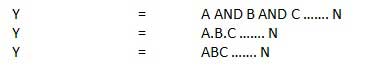
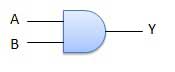
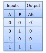
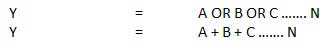
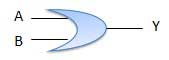
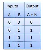
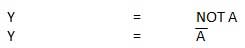
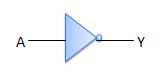
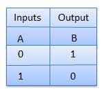
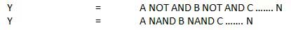
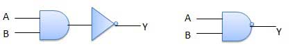
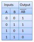
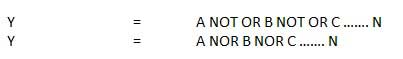
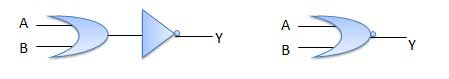
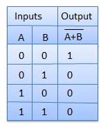
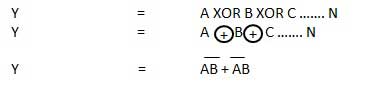
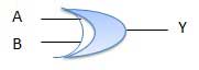
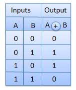
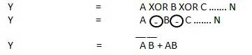
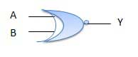
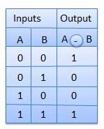


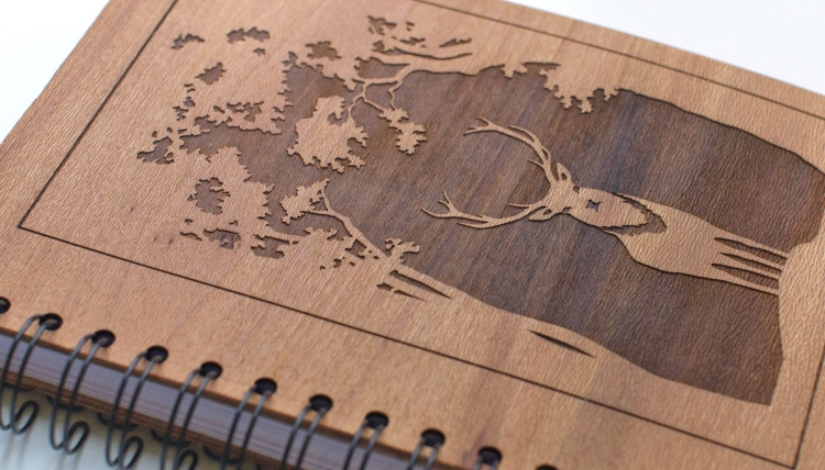


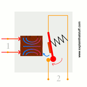
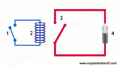

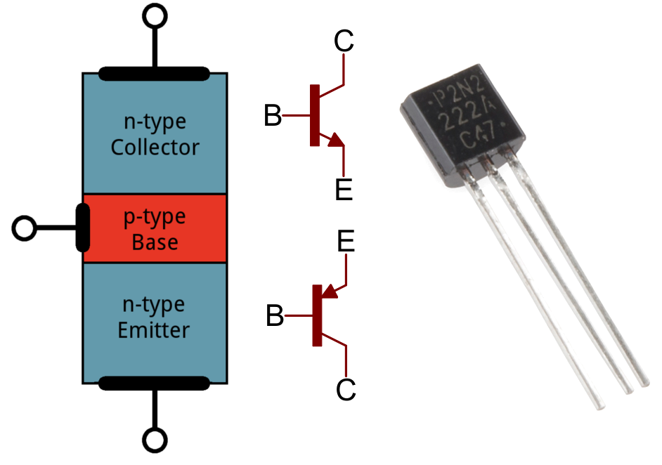
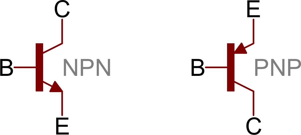
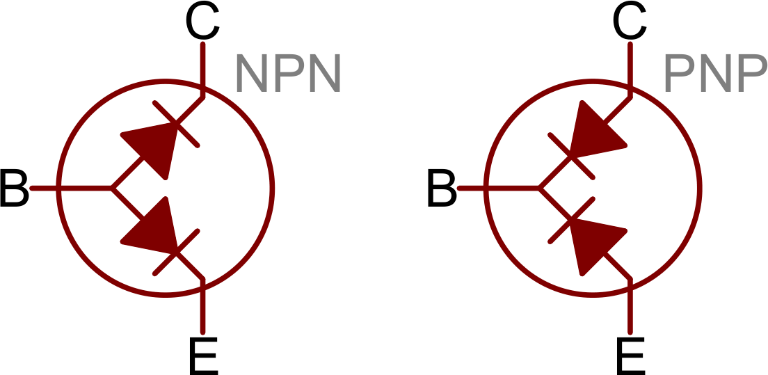
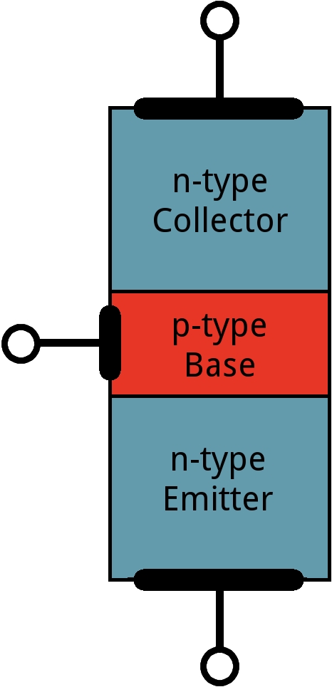
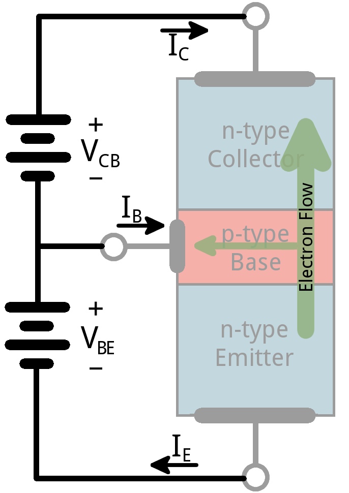
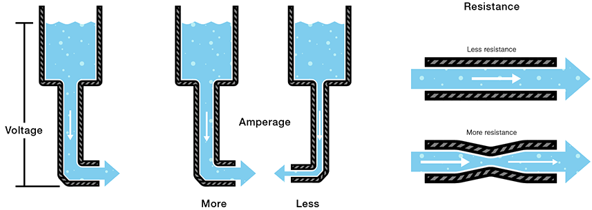


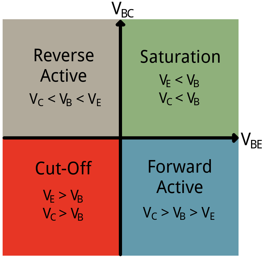
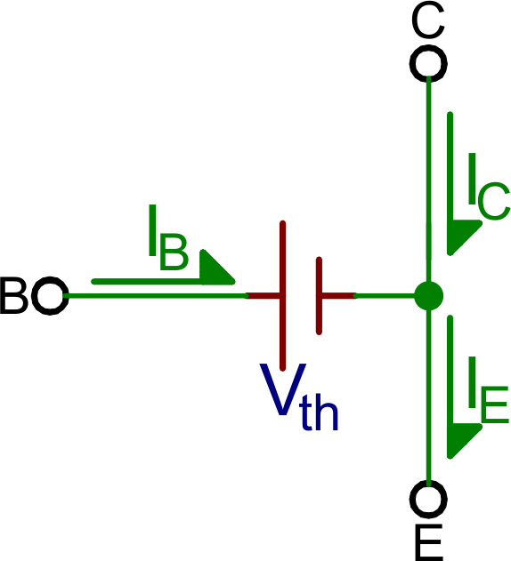
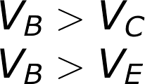
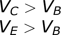
 V_{B} > V_{E}”/>
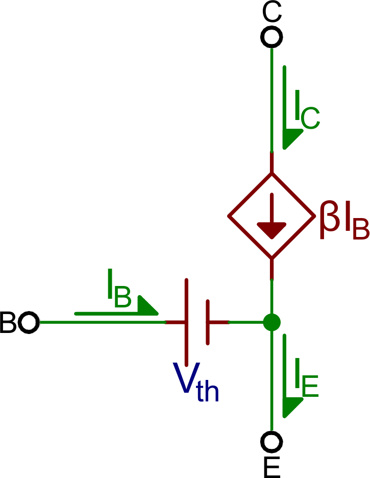

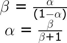

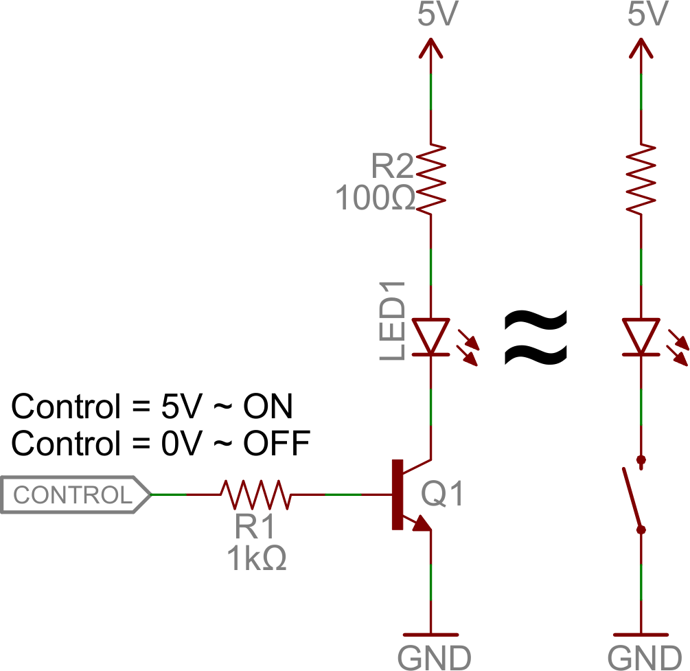
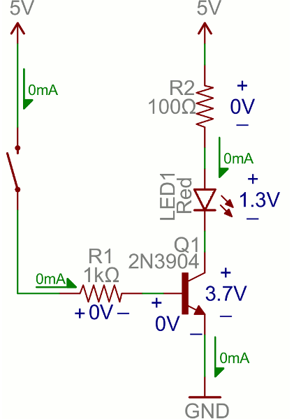
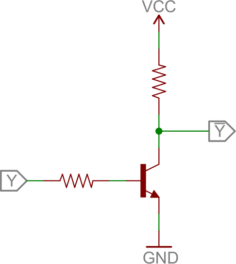
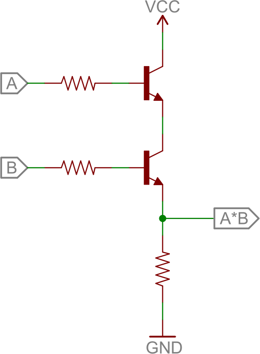
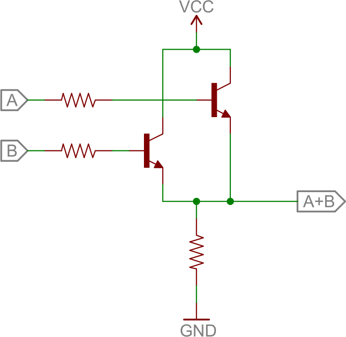
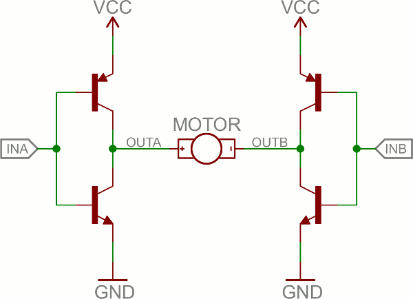
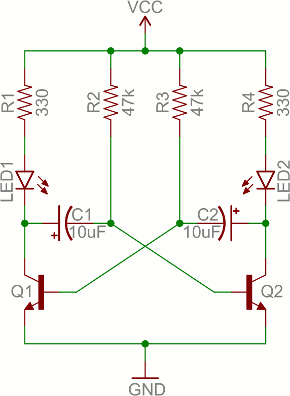
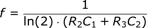
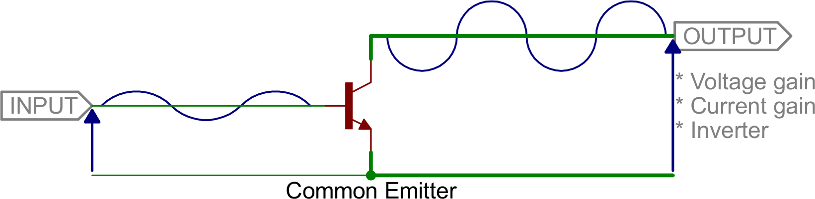
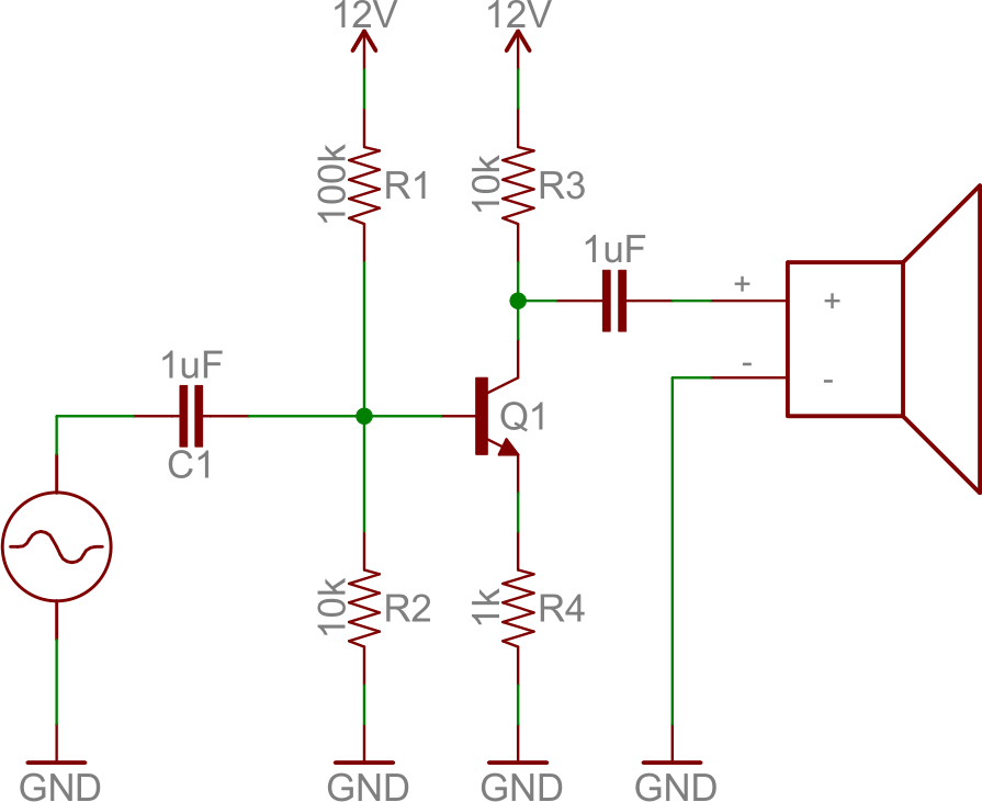

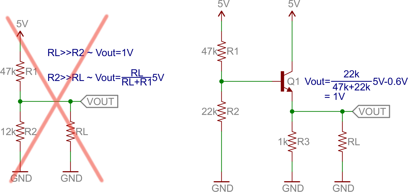
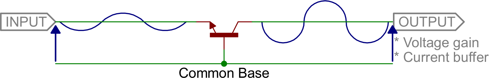
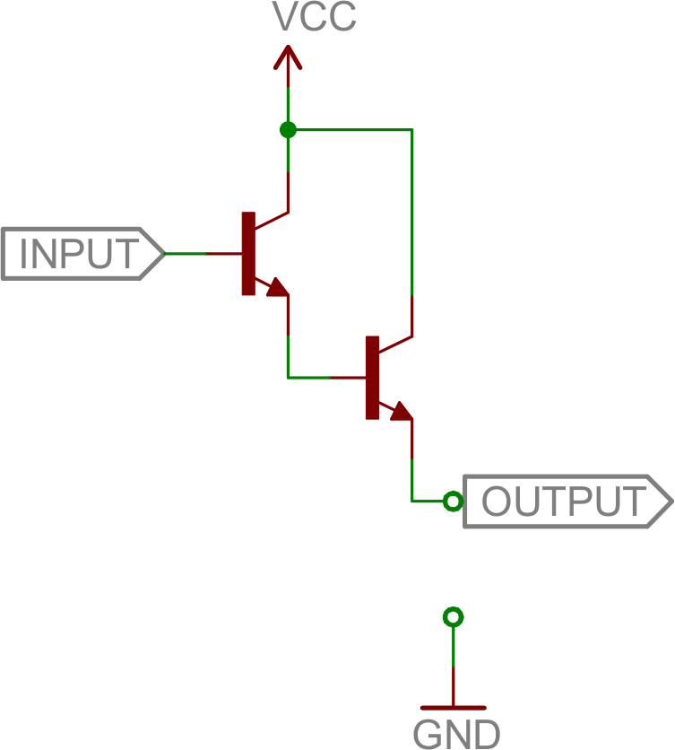
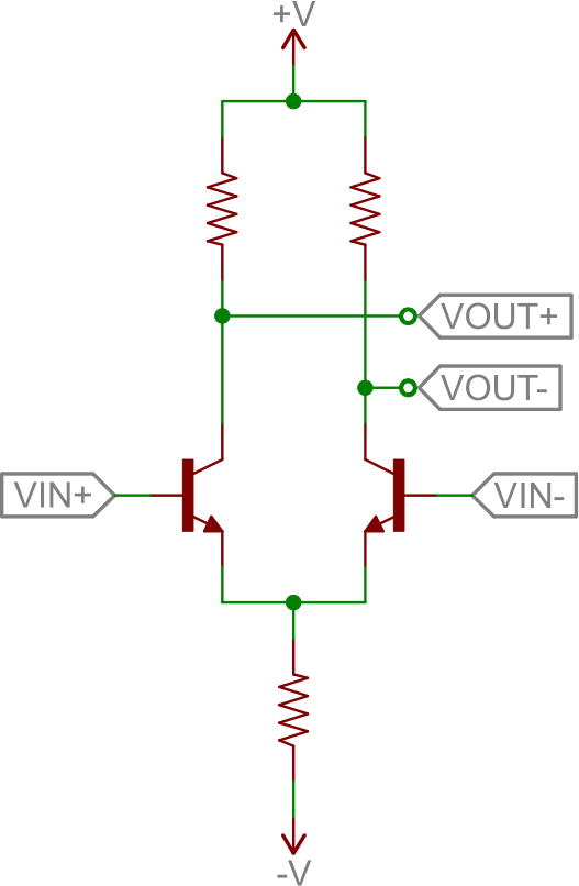
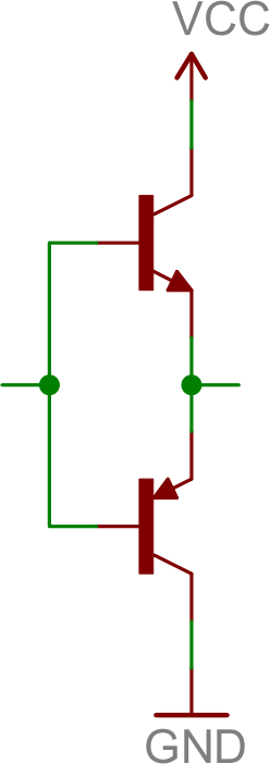
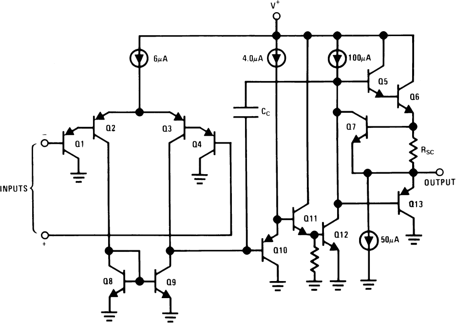
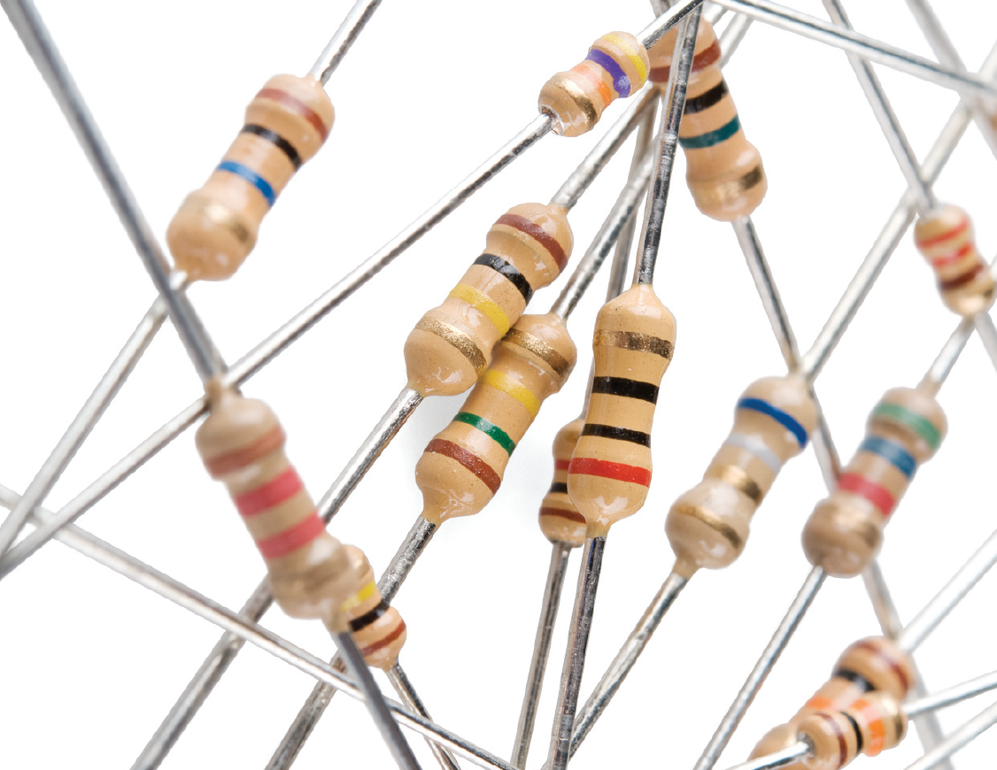
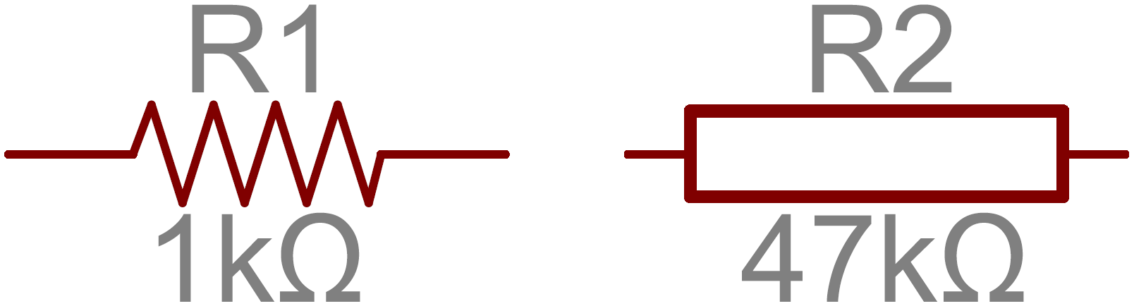
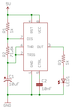
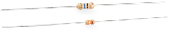

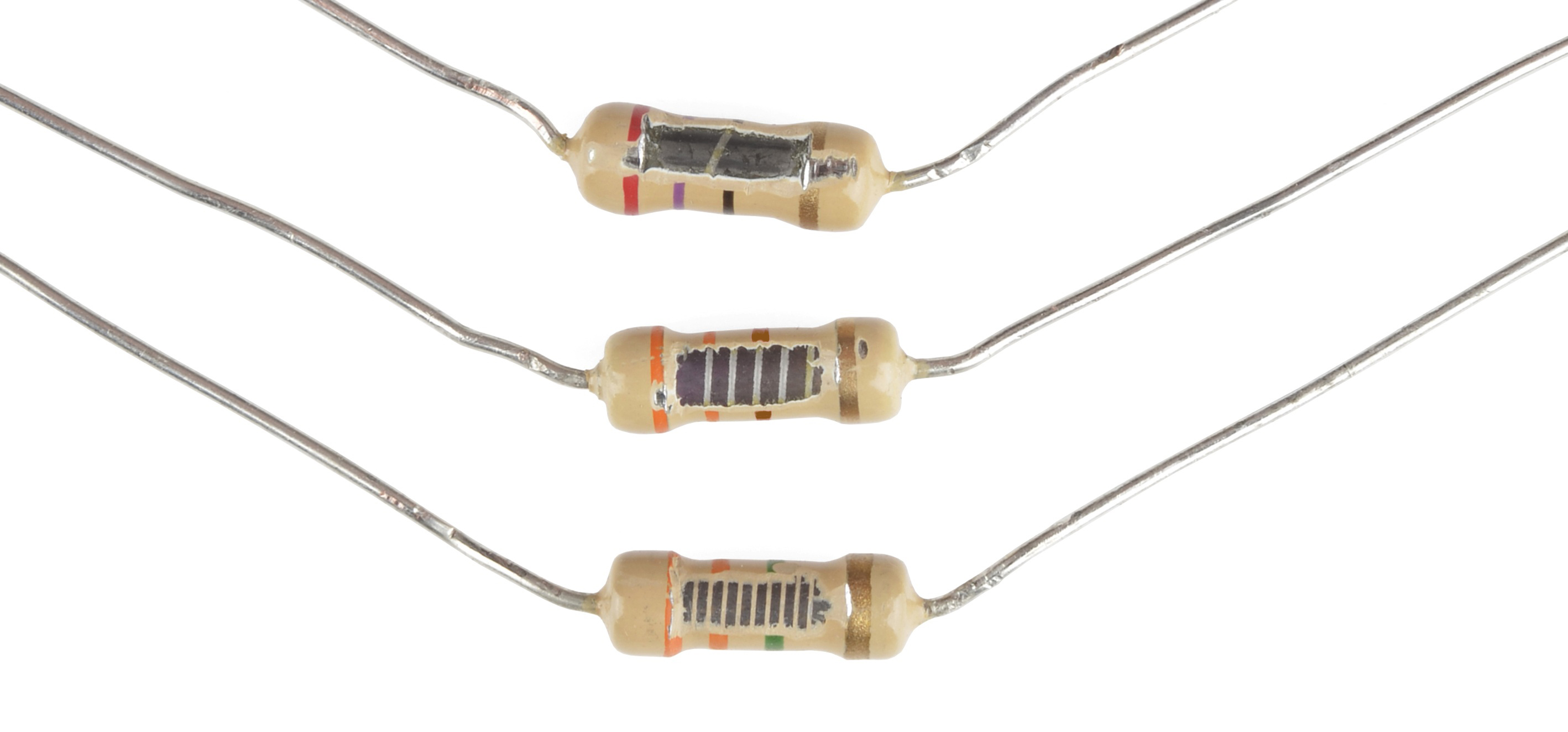
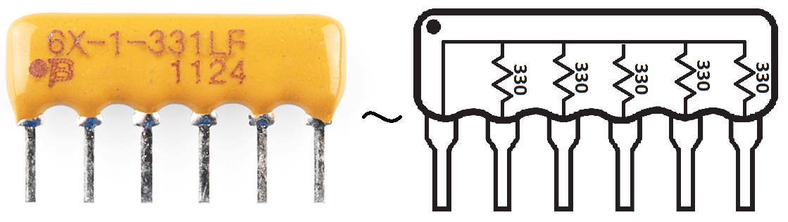
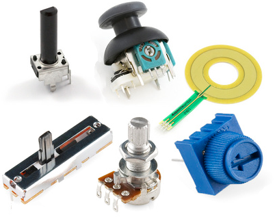
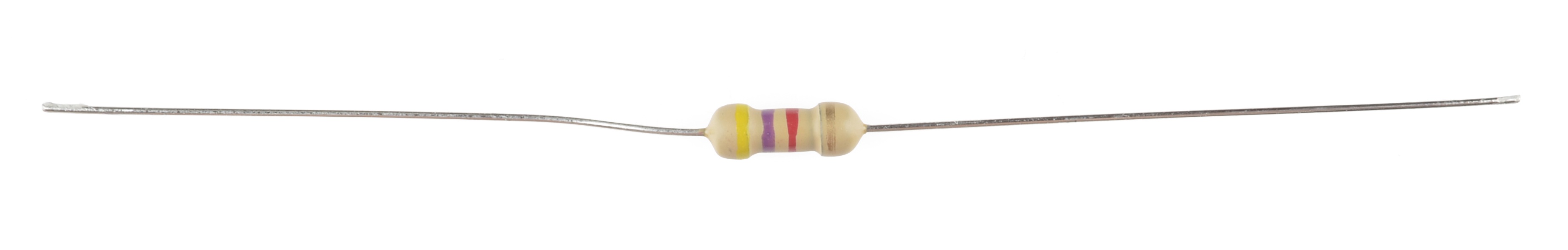
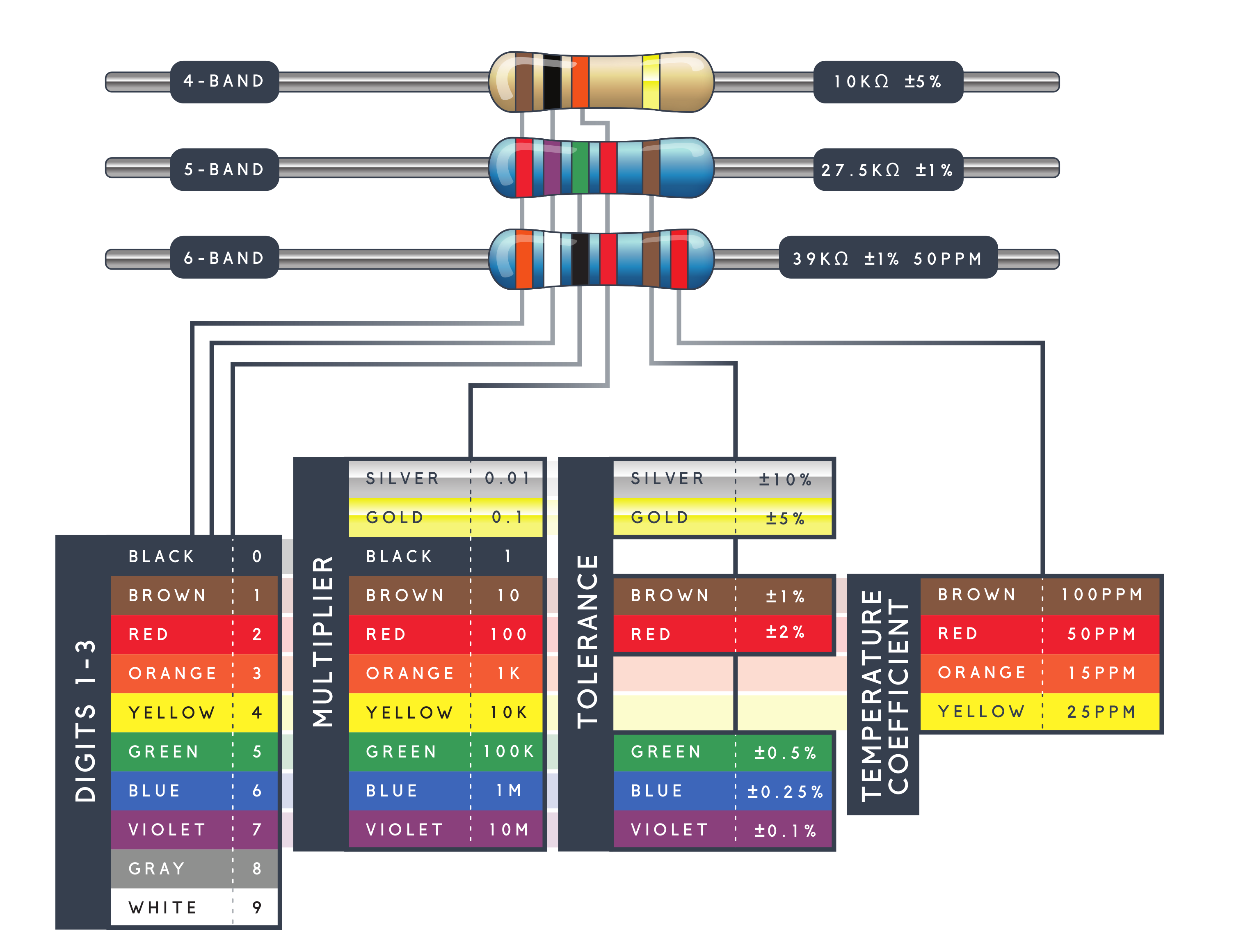
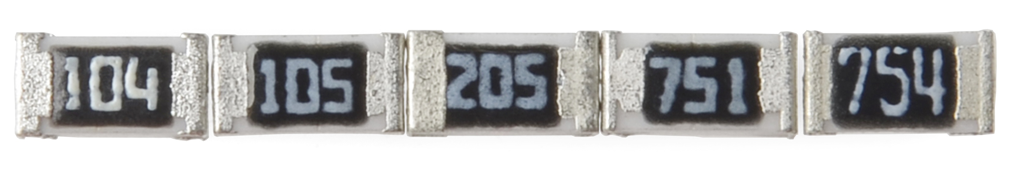
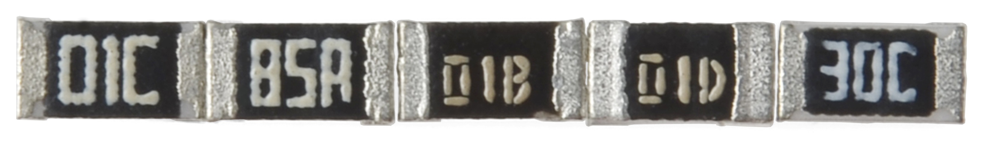
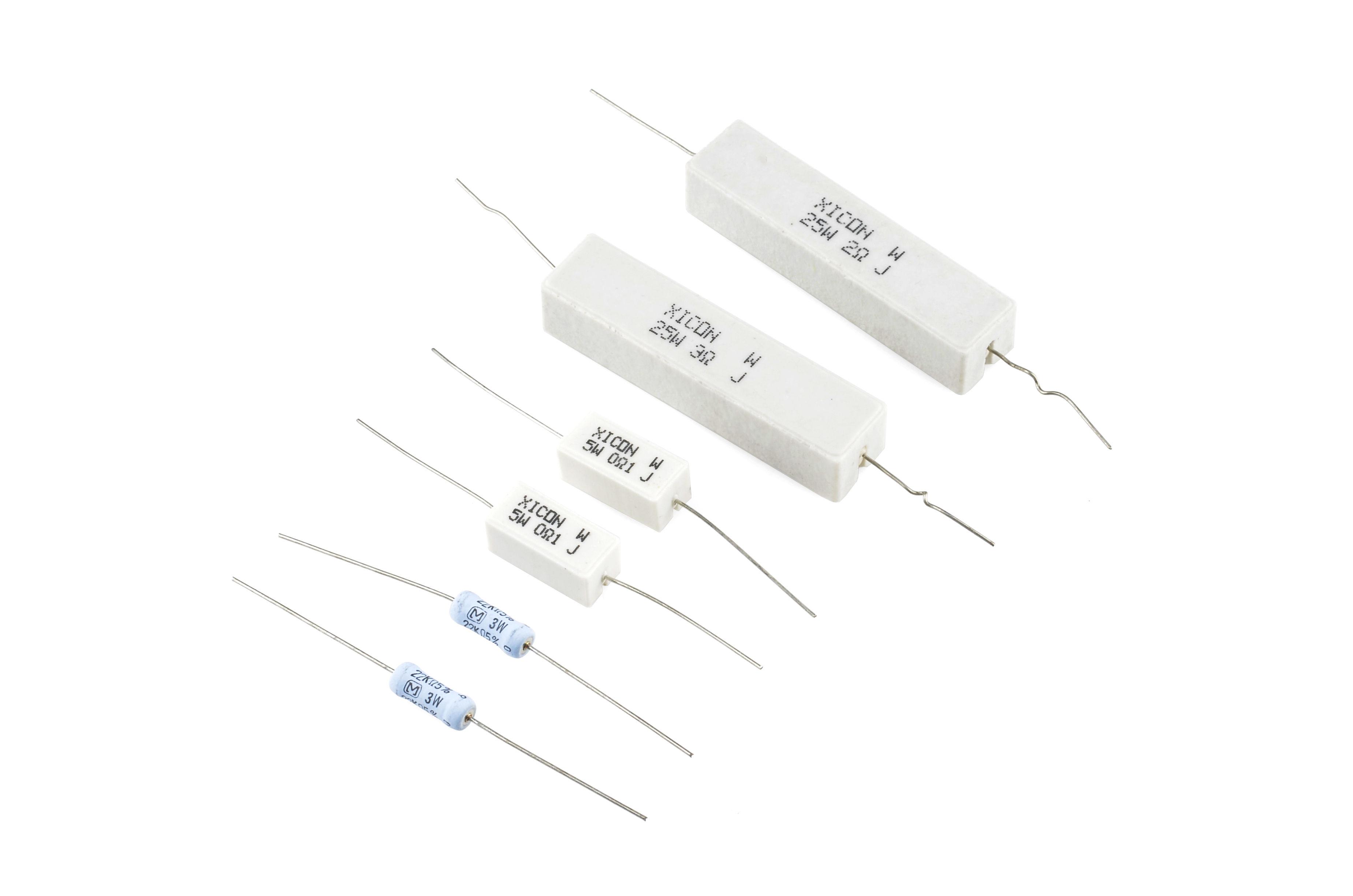

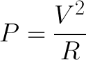


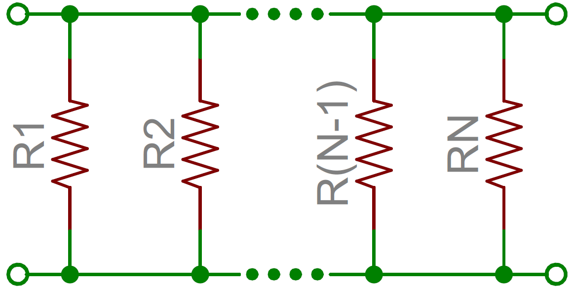
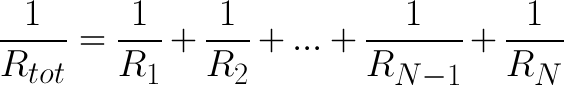
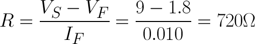
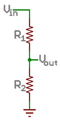
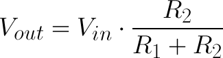
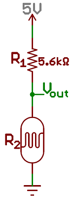
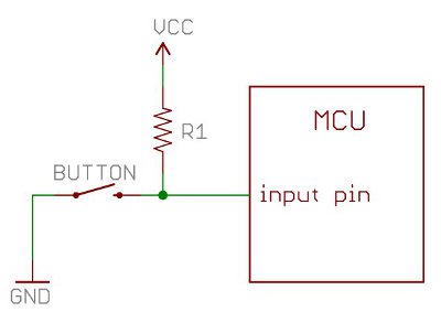
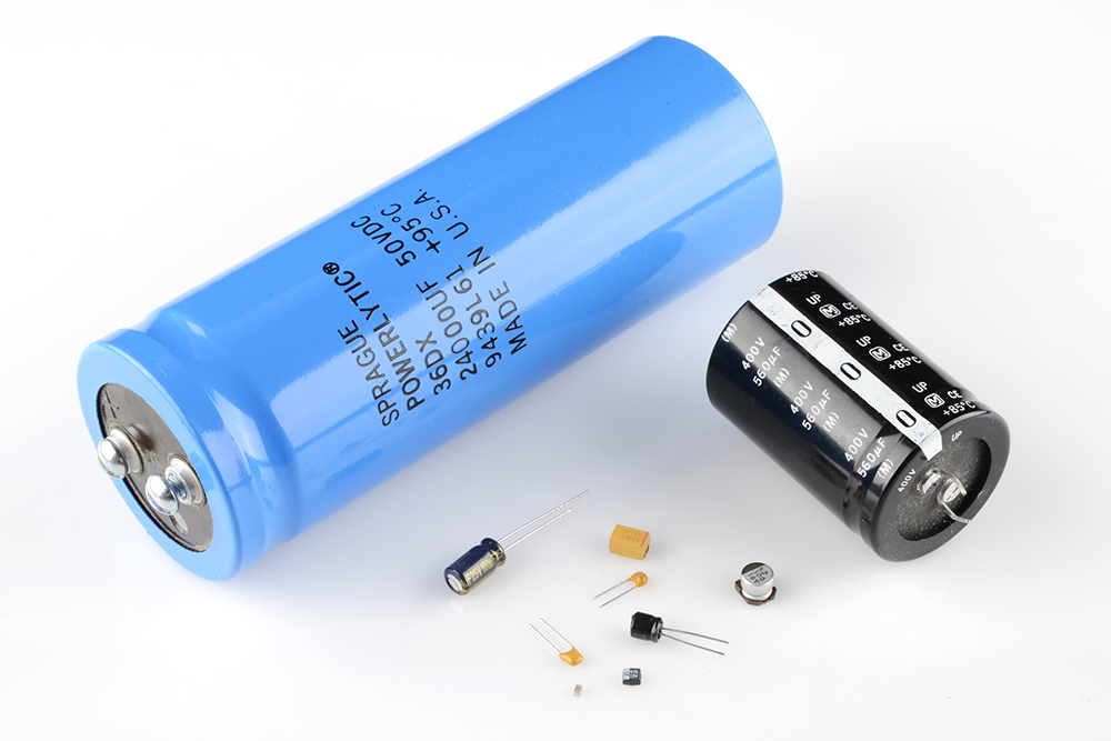
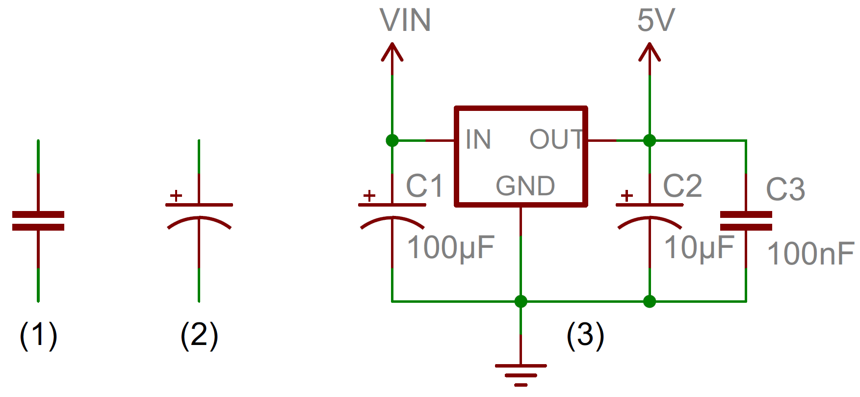
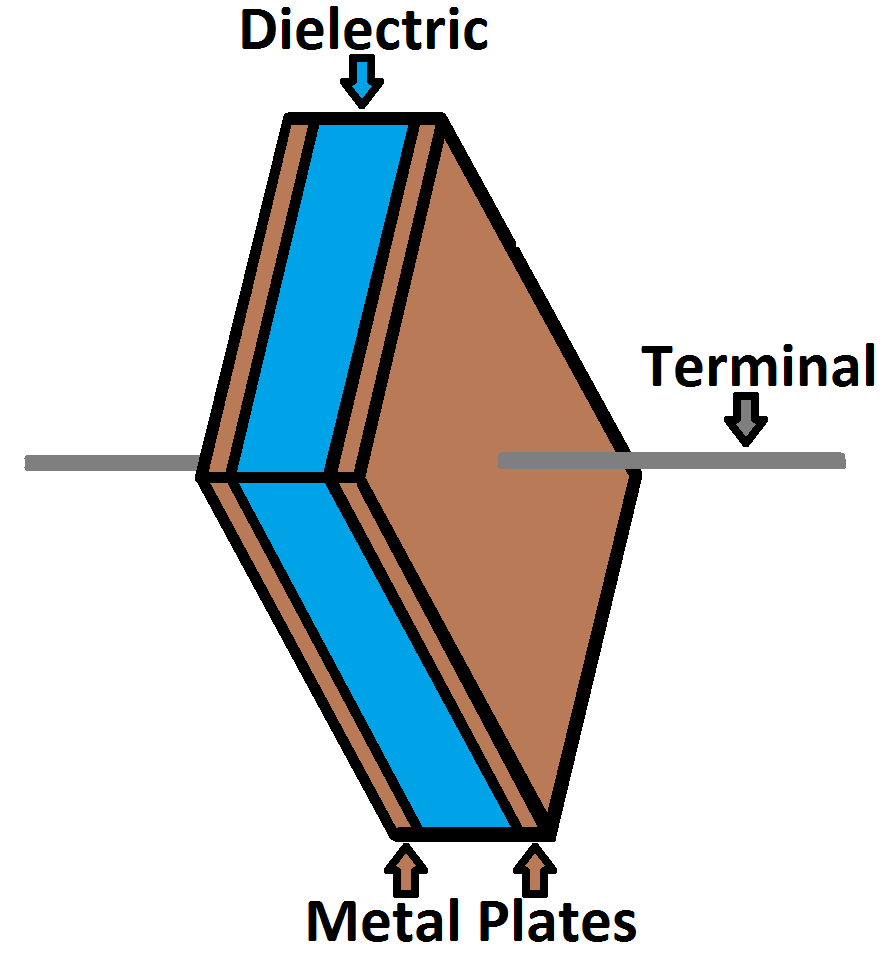
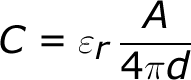
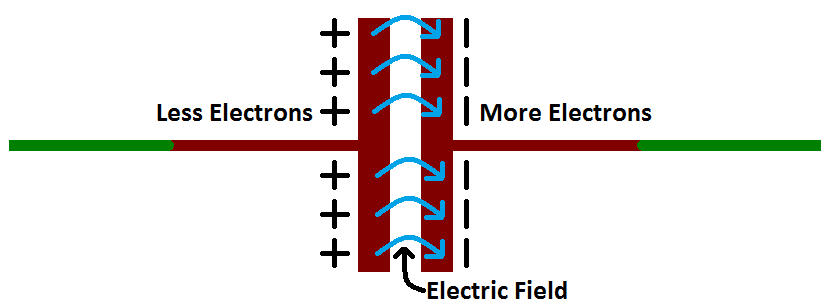
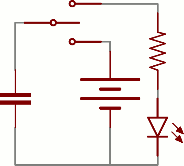

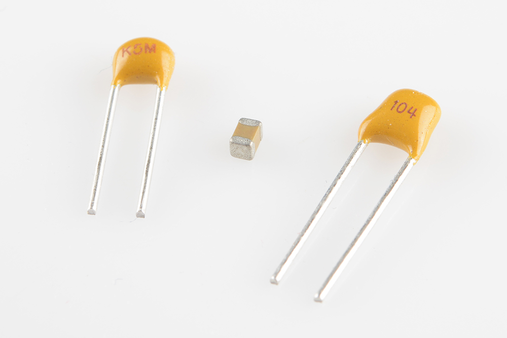
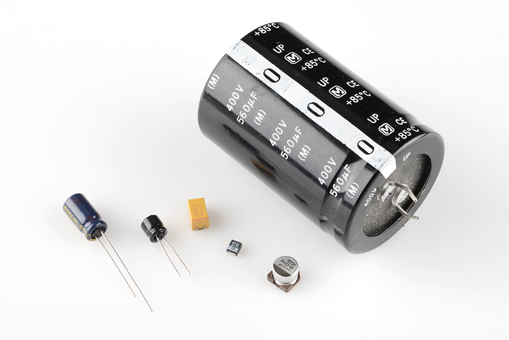
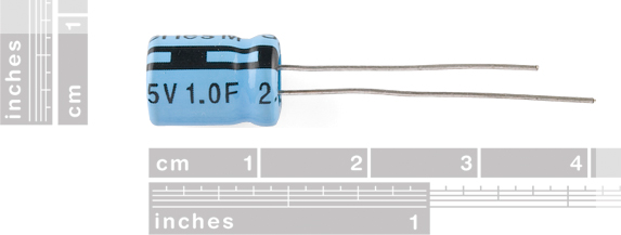
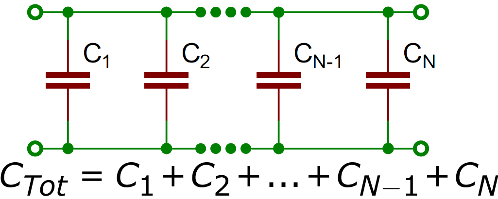
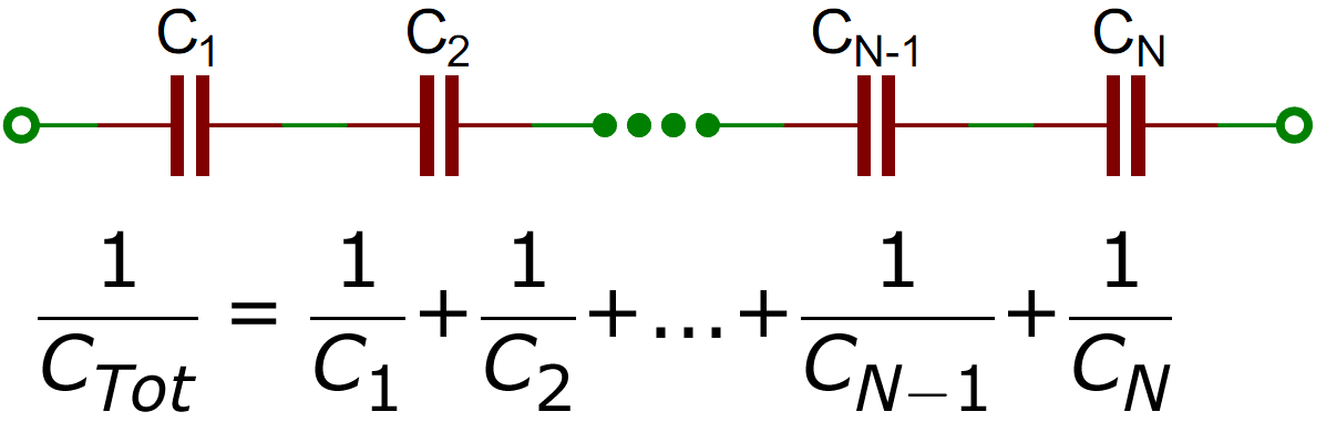
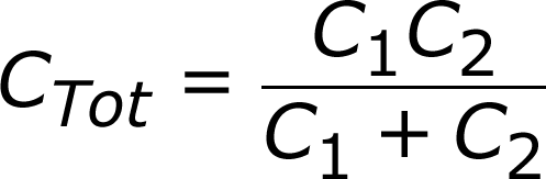
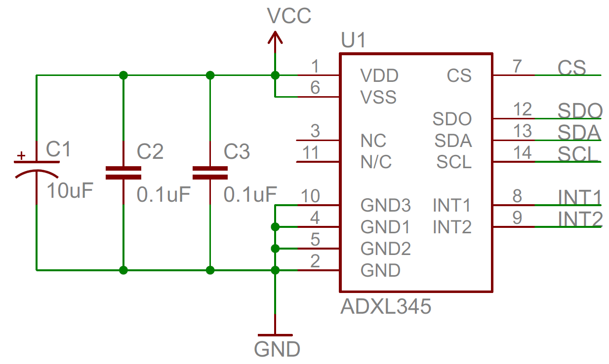
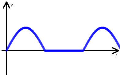
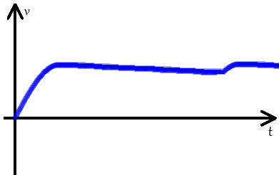

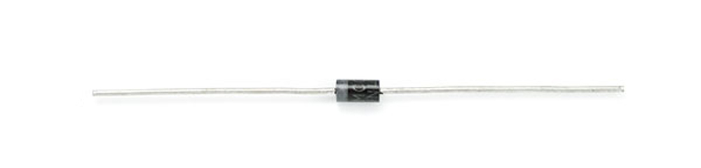
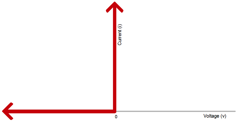
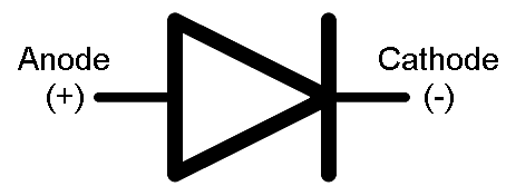
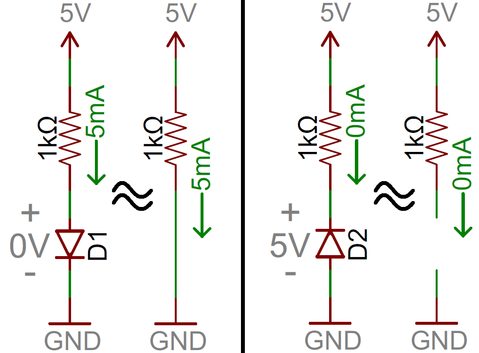
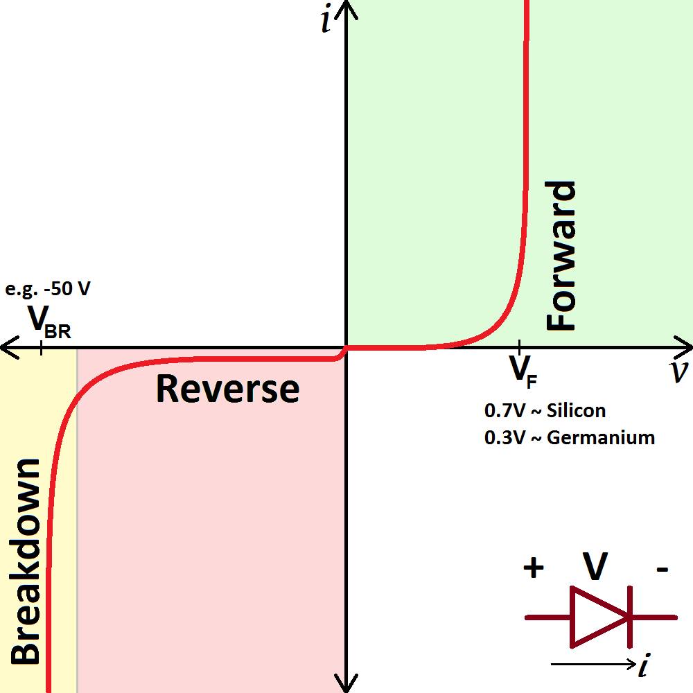
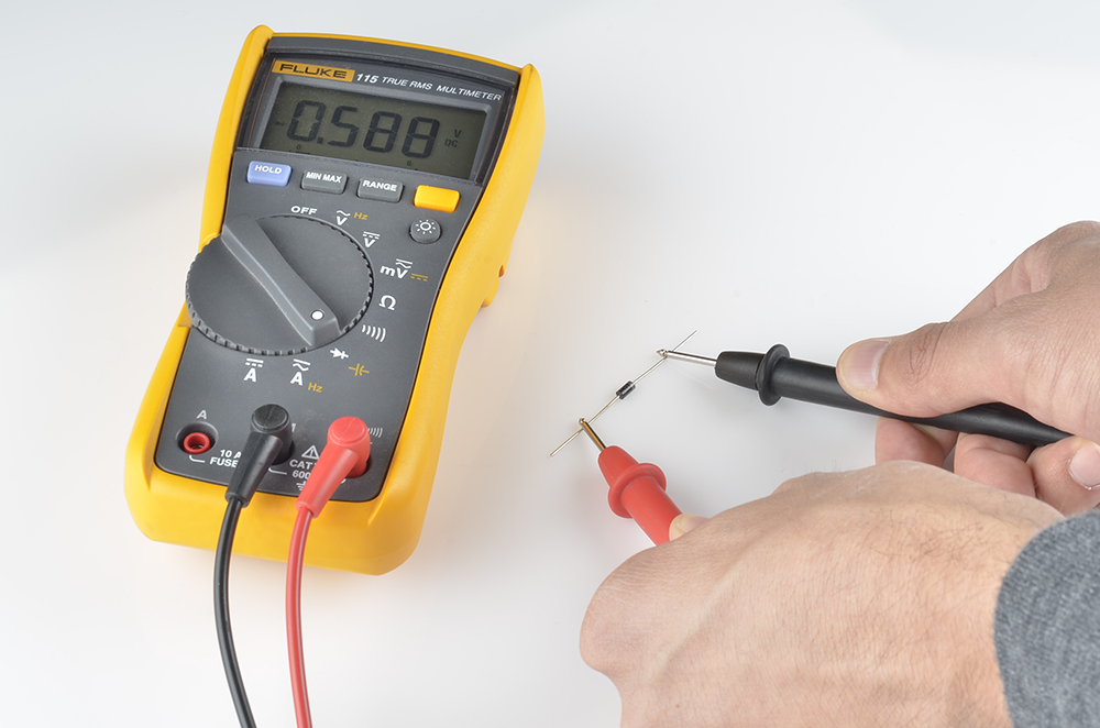
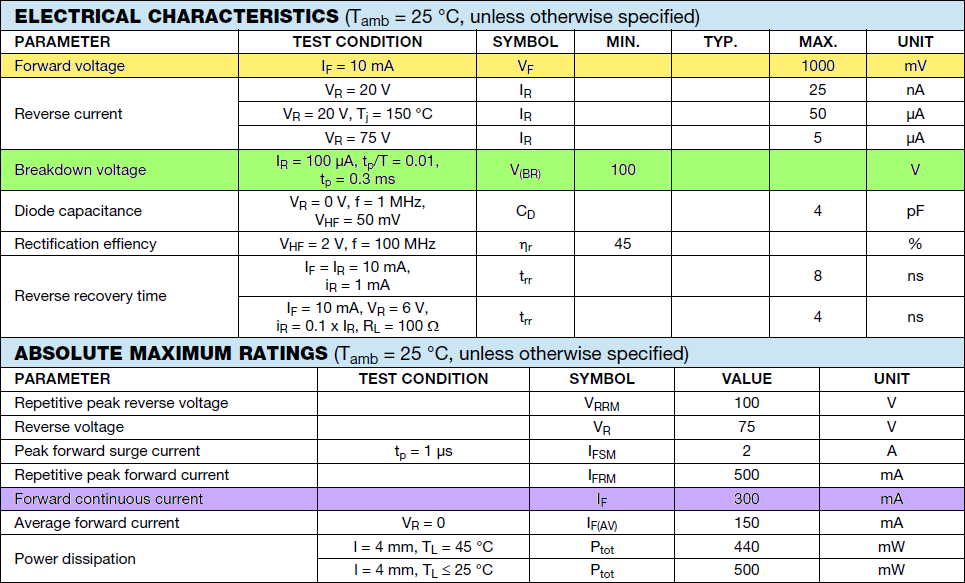
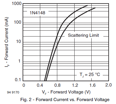
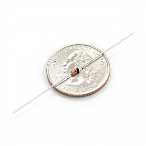
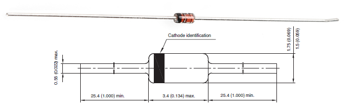
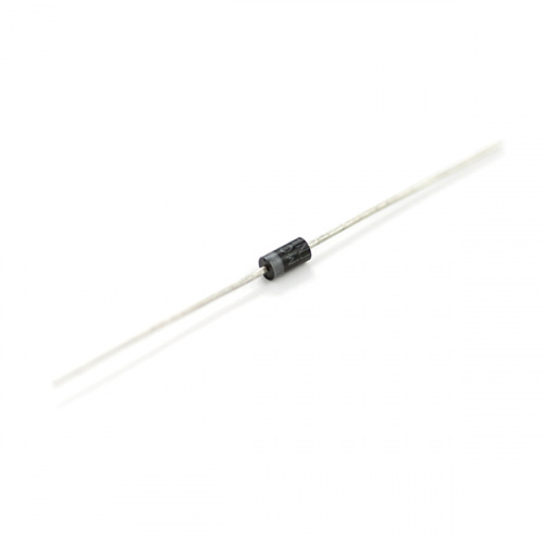
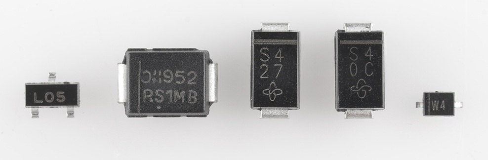

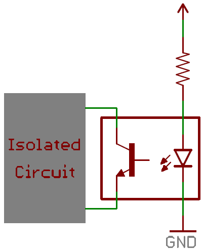

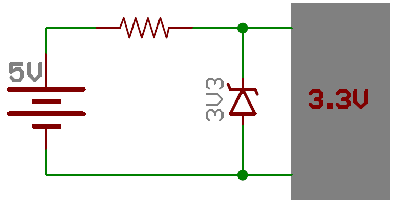
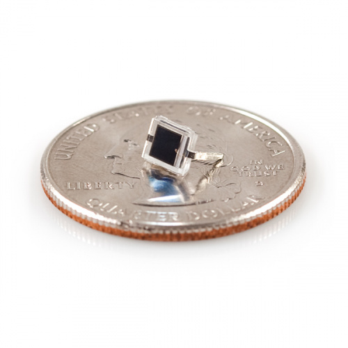
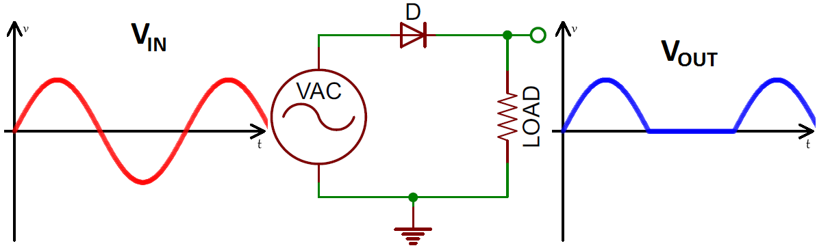
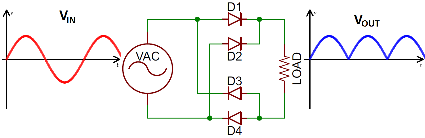
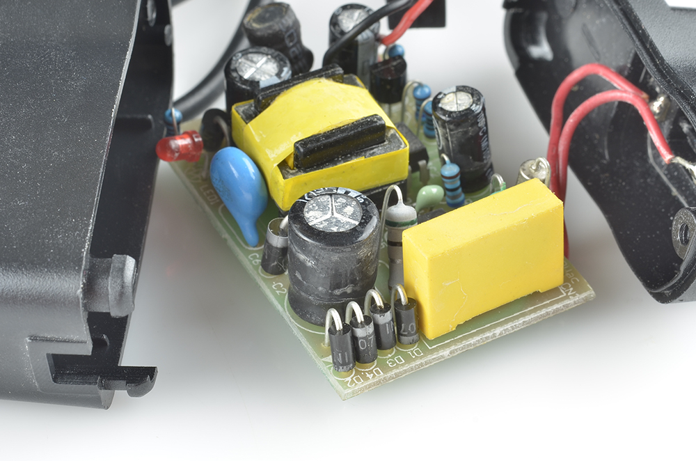

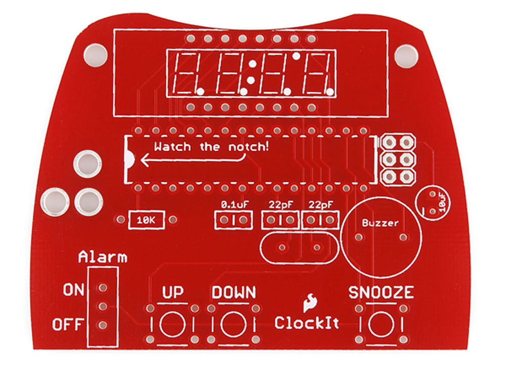
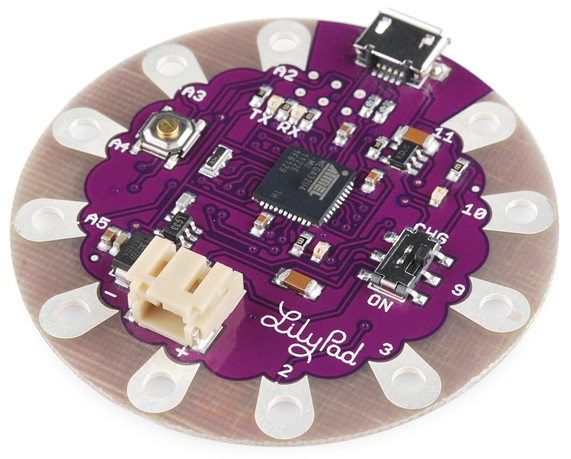
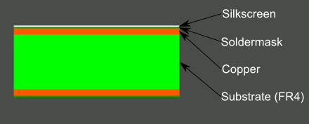
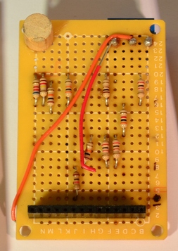
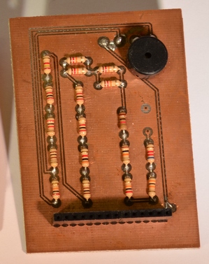
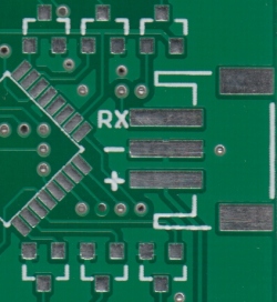
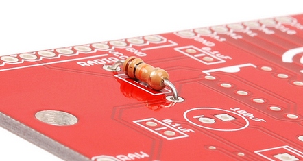
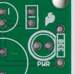
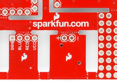
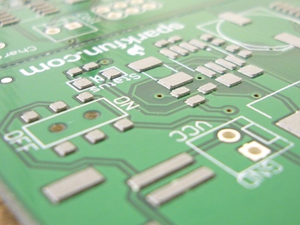
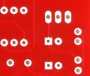
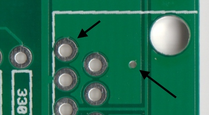
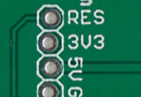
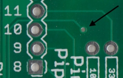
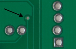